TPS2561A-Q1 Dual Channel Precision Automotive Adjustable Current-Limited Power Switches
1 Features
- AEC-Q100 Qualified
- Device HBM ESD Classification Level H2
- Device CDM ESD Classification Level C5
- Two separate current limiting channels
- Meets USB Current-Limiting Requirements
- Adjustable Current Limit, 250 mA–2.8 A (Typ.)
- Accurate 2.1A Min / 2.5A Max Setting
- Fast Short Circuit Response - 3.5-μs (typ)
- Two 44-mΩ High-Side MOSFETs
- Operating Range: 2.5 V to 6.5 V
- 2-μA Maximum Standby Supply Current
- Built-in Soft-Start
- 15 kV / 8 kV System-Level ESD Capable
2 Applications
Automotive USB Charging Ports
3 Description
The TPS2561A-Q1 is dual-channel power-distribution switch intended for automotive applications where precision current limiting is required or heavy capacitive loads and short circuits are encountered. These devices offer a programmable current-limit threshold between 250 mA and 2.8 A (typ) per channel via an external resistor. The power-switch rise and fall times are controlled to minimize current surges during turn on/off.
Each channel of the TPS2561A-Q1 devices limits the output current to a safe level by switching into a constant-current mode when the output load exceeds the current-limit threshold. The FAULTx logic output for each channel independently asserts low during overcurrent and over temperature conditions.
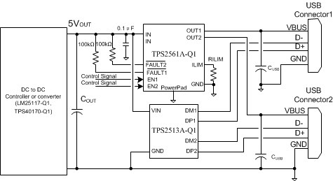
Use with the TPS2511-Q or TPS2513A-Q1 for a low loss, automotive qualified, USB Charging Port Solution capable of charging all of today's popular phones and tablets.
Device Information
| PART NUMBER | PACKAGE | BODY SIZE (NOM) |
|---|---|---|
| TPS2561A-Q1 | SON (10) | 3.00mm x 3.00mm |
Typical Application as Power Switch of Dual Port Automotive USB Charge Port Solution
4 Revision History
Changes from * Revision (March 2014) to A Revision
- Changed Feature From: Accurate 2.1A Min / 2.5A Max Setting (Including Resistor) To: Accurate 2.1A Min / 2.5A Max SettingGo
- Changed IOS, Current-limit. to include additional RILIM values. Go
- Changed Equation 1Go
- Changed the Designing Above a Minimum Current Limit sectionGo
- Changed the Designing Below a Maximum Current Limit sectionGo
5 Device Comparison Table
| DEVICE | MAXIMUM OPERATING CURRENT (A) | OUTPUTS | ENABLES | TYPICAL RDS(on) (mΩ) | PACKAGE |
|---|---|---|---|---|---|
| TPS2556-Q1 | 5 | 1 | Active-low | 22 | SON-8 (DRB) |
| TPS2557-Q1 | 5 | 1 | Active-high | 22 | SON-8 (DRB) |
| TPS2561A-Q1 | 2.5 | 2 | Active-high | 44 | SON-10 (DRC) |
6 Pin Functions and Configurations
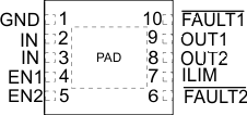
Pin Functions
| PIN | I/O | DESCRIPTION | |
|---|---|---|---|
| NAME | NUMBER | ||
| EN1 | 4 | I | Enable input, logic high turns on channel one power switch |
| EN2 | 5 | I | Enable input, logic high turns on channel two power switch |
| GND | 1 | Ground connection; connect externally to PowerPAD | |
| IN | 2, 3 | I | Input voltage; connect a 0.1 μF or greater ceramic capacitor from IN to GND as close to the IC as possible. |
| FAULT1 | 10 | O | Active-low open-drain output, asserted during overcurrent or overtemperature condition on channel one. |
| FAULT2 | 6 | O | Active-low open-drain output, asserted during overcurrent or overtemperature condition on channel two |
| OUT1 | 9 | O | Power-switch output for channel one |
| OUT2 | 8 | O | Power-switch output for channel two |
| ILIM | 7 | O | External resistor used to set current-limit threshold; recommended 20 kΩ ≤ RILIM ≤ 187 kΩ. |
| PowerPAD™ | PAD | Internally connected to GND; used to heat-sink the part to the circuit board traces. Connect PowerPAD to GND pin externally. | |
7 Specifications
7.1 Absolute Maximum Ratings
over operating free-air temperature range unless otherwise noted(1)(2)| MIN | MAX | UNIT | |||
|---|---|---|---|---|---|
| Voltage range on IN, OUTx, ENx, ILIM, FAULTx | –0.3 | 7 | V | ||
| Voltage range from IN to OUTx | –7 | 7 | V | ||
| Continuous output current | Internally Limited | ||||
| Continuous FAULTx sink current | 25 | mA | |||
| ILIM source current | Internally Limited | mA | |||
| TJ | Maximum junction temperature | –40 | Internally Limited | °C | |
7.2 Handling Ratings
| MIN | MAX | UNIT | |||
|---|---|---|---|---|---|
| TSTG | Storage temperature range | -65 | 150 | °C | |
| VESD(1) | Human Body Model (HBM) | AEC-Q100 Classification Level H2 | 2 | kV | |
| Charged Device Model (CDM) | AEC-Q100 Classification Level C5 | 750 | V | ||
| System level (contact/air) | 8/15(2) | kV | |||
7.3 Recommended Operating Conditions
| MIN | MAX | UNIT | |||
|---|---|---|---|---|---|
| VIN | Input voltage, IN | 2.5 | 6.5 | V | |
| VENx | Enable voltage | 0 | 6.5 | V | |
| VIH | High-level input voltage on ENx | 1.1 | V | ||
| VIL | Low-level input voltage on ENx | 0.66 | |||
| IOUTx | Continuous output current per channel, OUTx | 0 | 2.5 | A | |
| Continuous FAULTx sink current | 0 | 10 | mA | ||
| TJ | Operating junction temperature | –40 | 125 | °C | |
| RILIM | Recommended resistor limit range | 20 | 187 | kΩ | |
7.4 Thermal Information(1)
| THERMAL METRIC | TPS2561A-Q1 | UNIT | |
|---|---|---|---|
| DRC (10 TERMINALS) | |||
| θJA | Junction-to-ambient thermal resistance | 38.1 | °C/W |
| θJCtop | Junction-to-case (top) thermal resistance | 40.5 | |
| θJB | Junction-to-board thermal resistance | 13.6 | |
| ψJT | Junction-to-top characterization parameter | 0.6 | |
| ψJB | Junction-to-board characterization parameter | 13.7 | |
| θJCbot | Junction-to-case (bottom) thermal resistance | 3.4 | |
7.5 Electrical Characteristics
over recommended operating conditions, VENx = VIN (unless otherwise noted)| PARAMETER | TEST CONDITIONS(1) | MIN | TYP | MAX | UNIT | ||||
|---|---|---|---|---|---|---|---|---|---|
| POWER SWITCH | |||||||||
| rDS(on) | Static drain-source on-state resistance per channel, IN to OUTx | TJ = 25°C | 44 | 50 | mΩ | ||||
| –40°C ≤TJ ≤125 °C | 70 | ||||||||
| tr | Rise time, output | VIN = 6.5 V | CLx = 1 μF, RLx = 100 Ω, (see Figure 9) |
1.5 | 3 | 4 | ms | ||
| VIN = 2.5 V | 0.5 | 2 | 3 | ||||||
| tf | Fall time, output | VIN = 6.5 V | 0.5 | 0.8 | 1.0 | ||||
| VIN = 2.5 V | 0.3 | 0.6 | 0.8 | ||||||
| ENABLE INPUT EN | |||||||||
| Enable pin turn on/off threshold | 0.66 | 1.1 | V | ||||||
| Hysteresis | 55(2) | mV | |||||||
| IEN | Input current | VENx = 0 V or 6.5 V | –0.5 | 0.5 | μA | ||||
| ton | Turnon time | CLx = 1 μF, RLx = 100 Ω, (see Figure 9) | 9 | ms | |||||
| toff | Turnoff time | 6 | ms | ||||||
| CURRENT LIMIT | |||||||||
| IOS | Current-limit (see Figure 11) | OUTx connected to GND | RILIM = 20 kΩ | 2560 | 2750 | 2980 | mA | ||
| RILIM = 24.3 kΩ | 2100 | 2250 | 2500 | ||||||
| RILIM = 61.9 kΩ | 800 | 900 | 1005 | ||||||
| RILIM = 100 kΩ | 470 | 560 | 645 | ||||||
| OUT1 and OUT2 connected to GND | RILIM = 47.5 kΩ | 2100 | 2300 | 2500 | |||||
| tIOS | Response time to short circuit | VIN = 5 V (see Figure 10) | 3.5(2) | μs | |||||
| SUPPLY CURRENT | |||||||||
| IIN(off) | Supply current, low-level output | VIN = 6.5 V, No load on OUTx, VENx = 0 V | 0.1 | 2.0 | μA | ||||
| IIN(on) | Supply current, high-level output | VIN = 6.5 V, No load on OUT | RILIM = 20 kΩ | 100 | 125 | μA | |||
| RILIM = 100 kΩ | 85 | 110 | μA | ||||||
| IREV | Reverse leakage current | VOUTx = 6.5 V, VIN = 0 V | TJ = 25°C | 0.01 | 1.0 | μA | |||
| UNDERVOLTAGE LOCKOUT | |||||||||
| VUVLO | Low-level input voltage, IN | VIN rising | 2.35 | 2.45 | V | ||||
| Hysteresis, IN | TJ = 25°C | 35(2) | mV | ||||||
| FAULTx FLAG | |||||||||
| VOL | Output low voltage, FAULTx | IFAULTx = 1 mA | 180 | mV | |||||
| Off-state leakage | VFAULTx = 6.5 V | 1 | μA | ||||||
| FAULTx deglitch | FAULTx assertion or de-assertion due to overcurrent condition | 6 | 9 | 13 | ms | ||||
| THERMAL SHUTDOWN | |||||||||
| Thermal shutdown threshold, OTSD2 | 155 | °C | |||||||
| Thermal shutdown threshold in current-limit, OTSD | 135 | °C | |||||||
| Hysteresis | 20(2) | °C | |||||||
7.6 Typical Characteristics


| RLIM = 20 kΩ |


| RLIM = 61.9 kΩ |


| RLIM = 20 kΩ |

| RLIM = 100 kΩ |

| RLIM = 20 kΩ |