JAJSRT9 October 2023 TPS25730
PRODUCTION DATA
- 1
- 1 特長
- 2 アプリケーション
- 3 概要
- 4 Device Comparison Table
- 5 Pin Configuration and Functions
-
6 Specifications
- 6.1 Absolute Maximum Ratings
- 6.2 ESD Ratings
- 6.3 Recommended Operating Conditions
- 6.4 Recommended Capacitance
- 6.5 Thermal Information
- 6.6 Power Supply Characteristics
- 6.7 Power Consumption
- 6.8 PPHV Power Switch Characteristics - TPS25730D
- 6.9 PP_EXT Power Switch Characteristics - TPS25730S
- 6.10 Power Path Supervisory
- 6.11 CC Cable Detection Parameters
- 6.12 CC PHY Parameters
- 6.13 Thermal Shutdown Characteristics
- 6.14 ADC Characteristics
- 6.15 Input/Output (I/O) Characteristics
- 6.16 I2C Requirements and Characteristics
- 6.17 Typical Characteristics
- 7 Parameter Measurement Information
-
8 Detailed Description
- 8.1 Overview
- 8.2 Functional Block Diagram
- 8.3
Feature Description
- 8.3.1 USB-PD Physical Layer
- 8.3.2 Power Management
- 8.3.3 Power Paths
- 8.3.4 Cable Plug and Orientation Detection
- 8.3.5 Overvoltage Protection (CC1, CC2)
- 8.3.6 Default Behavior Configuration (ADCIN1, ADCIN2)
- 8.3.7 ADC
- 8.3.8 Digital Interfaces
- 8.3.9 Digital Core
- 8.3.10 I2C Interface
- 8.3.11 Minimum Voltage Configuration
- 8.3.12 Maximum Voltage Configuration
- 8.3.13 Sink Current Configuration
- 8.3.14 Autonegotiate Sink Minimum Power
- 8.3.15 Extended Sink Capabilities Power Delivery Power
- 8.4 Device Functional Modes
- 8.5 Schottky for Current Surge Protection
- 8.6 Thermal Shutdown
- 9 Application and Implementation
- 10Device and Documentation Support
- 11Revision History
- 12Mechanical, Packaging, and Orderable Information
パッケージ・オプション
メカニカル・データ(パッケージ|ピン)
サーマルパッド・メカニカル・データ
- RSM|32
発注情報
8.4.1 Power States
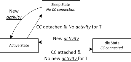
The TPS25730 can operate in one of three different power states: Active, Idle, or Sleep. The Modern Standby mode is a special case of the Idle mode. The functionality available in each state is summarized in Table 8-9. The device automatically transitions between the three power states based on the circuits that are active and required. See Figure 8-26. In the Sleep state, the TPS25730 detects a Type-C connection. Transitioning between the Active mode to Idle mode requires a period of time (T) without any of the following activity:
- Incoming USB PD message
- Change in CC status
- GPIO input event
- I2C transactions
- Voltage alert
- Fault alert
 Figure 8-26 Flow
Diagram for Power States
Figure 8-26 Flow
Diagram for Power StatesTable 8-9 Power
Consumption States
| ACTIVE SINK MODE(3) | IDLE SINK MODE | MODERN STANDBY SINK MODE(2) | SLEEP MODE(1) | |
|---|---|---|---|---|
| PP_HV (TPS25730D) | enabled | enabled | disabled | disabled |
| PP_EXT (TPS25730S) | enabled | enabled | disabled | disabled |
| external CC1 termination | Rp 3.0A | Rp 3.0A | open | open |
| external CC2 termination | open | open | open | open |
(1) This mode is used for:
IVIN_3V3,Sleep
(2) This mode is used for:
PMstbySnk
(3) This mode is used for:
IVIN_3V3,ActSnk