JAJSRT9 October 2023 TPS25730
PRODUCTION DATA
- 1
- 1 特長
- 2 アプリケーション
- 3 概要
- 4 Device Comparison Table
- 5 Pin Configuration and Functions
-
6 Specifications
- 6.1 Absolute Maximum Ratings
- 6.2 ESD Ratings
- 6.3 Recommended Operating Conditions
- 6.4 Recommended Capacitance
- 6.5 Thermal Information
- 6.6 Power Supply Characteristics
- 6.7 Power Consumption
- 6.8 PPHV Power Switch Characteristics - TPS25730D
- 6.9 PP_EXT Power Switch Characteristics - TPS25730S
- 6.10 Power Path Supervisory
- 6.11 CC Cable Detection Parameters
- 6.12 CC PHY Parameters
- 6.13 Thermal Shutdown Characteristics
- 6.14 ADC Characteristics
- 6.15 Input/Output (I/O) Characteristics
- 6.16 I2C Requirements and Characteristics
- 6.17 Typical Characteristics
- 7 Parameter Measurement Information
-
8 Detailed Description
- 8.1 Overview
- 8.2 Functional Block Diagram
- 8.3
Feature Description
- 8.3.1 USB-PD Physical Layer
- 8.3.2 Power Management
- 8.3.3 Power Paths
- 8.3.4 Cable Plug and Orientation Detection
- 8.3.5 Overvoltage Protection (CC1, CC2)
- 8.3.6 Default Behavior Configuration (ADCIN1, ADCIN2)
- 8.3.7 ADC
- 8.3.8 Digital Interfaces
- 8.3.9 Digital Core
- 8.3.10 I2C Interface
- 8.3.11 Minimum Voltage Configuration
- 8.3.12 Maximum Voltage Configuration
- 8.3.13 Sink Current Configuration
- 8.3.14 Autonegotiate Sink Minimum Power
- 8.3.15 Extended Sink Capabilities Power Delivery Power
- 8.4 Device Functional Modes
- 8.5 Schottky for Current Surge Protection
- 8.6 Thermal Shutdown
- 9 Application and Implementation
- 10Device and Documentation Support
- 11Revision History
- 12Mechanical, Packaging, and Orderable Information
パッケージ・オプション
メカニカル・データ(パッケージ|ピン)
サーマルパッド・メカニカル・データ
- RSM|32
発注情報
9.4.2.4 Routing VBUS, PPHV, VIN_3V3, LDO_3V3, LDO_1V5
On the top side, create pours for VBUS, and PPHV. Connect PPHV from the top layer to the bottom layer using at least 12, 8-mil hole and 16-mil diameter vias. See Figure 9-25 for the recommended via sizing. The via placement and copper pours are highlighted in Figure 9-26.
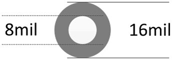 Figure 9-25 Recommended Minimum Via Sizing
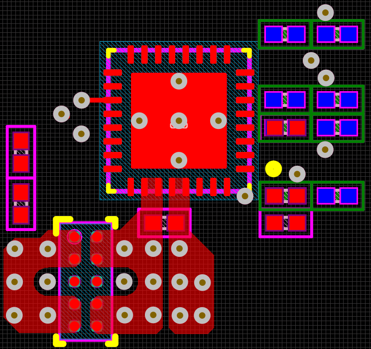 Figure 9-26 VBUS
Copper Pours and Via Placement
Figure 9-26 VBUS
Copper Pours and Via PlacementNext, VIN_3V3, LDO_3V3, and LDO_1V5 are routed to their respective decoupling capacitors. This action is highlighted in Figure 9-27.
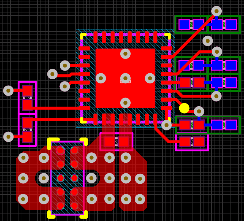 Figure 9-27 VIN_3V3,
LDO_3V3, and LDO_1V5 Routing
Figure 9-27 VIN_3V3,
LDO_3V3, and LDO_1V5 RoutingFigure 9-28 and Figure 9-29 show how to properly connect VSYS and the SYS_Gate control signals for the external N-FETs. The control signals can be routed on an internal layer using a 12-mil trace, and the trace going to VSYS must be as short as possible to minimize impedance, so placing a via directly on the high-voltage power path is ideal.
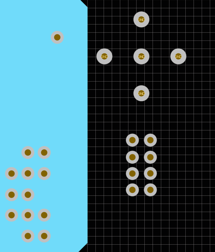 Figure 9-28 Top Polygon Pours
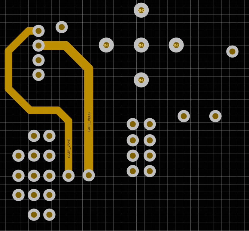 Figure 9-29 Bottom Polygon
Pours