JAJSRT9 October   2023 TPS25730

PRODUCTION DATA  

  1.   1
  2. 特長
  3. アプリケーション
  4. 概要
  5. Device Comparison Table
  6. Pin Configuration and Functions
  7. Specifications
    1. 6.1  Absolute Maximum Ratings
      1. 6.1.1 TPS25730D and TPS25730S - Absolute Maximum Ratings
      2. 6.1.2 TPS25730D - Absolute Maximum Ratings
      3. 6.1.3 TPS25730S - Absolute Maximum Ratings
    2. 6.2  ESD Ratings
    3. 6.3  Recommended Operating Conditions
      1. 6.3.1 TPS25730D - Recommended Operating Conditions
      2. 6.3.2 TPS25730S - Recommended Operating Conditions
    4. 6.4  Recommended Capacitance
    5. 6.5  Thermal Information
      1. 6.5.1 TPS25730D - Thermal Information
      2. 6.5.2 TPS25730S - Thermal Information
    6. 6.6  Power Supply Characteristics
    7. 6.7  Power Consumption
    8. 6.8  PPHV Power Switch Characteristics - TPS25730D
    9. 6.9  PP_EXT Power Switch Characteristics - TPS25730S
    10. 6.10 Power Path Supervisory
    11. 6.11 CC Cable Detection Parameters
    12. 6.12 CC PHY Parameters
    13. 6.13 Thermal Shutdown Characteristics
    14. 6.14 ADC Characteristics
    15. 6.15 Input/Output (I/O) Characteristics
    16. 6.16 I2C Requirements and Characteristics
    17. 6.17 Typical Characteristics
  8. Parameter Measurement Information
  9. Detailed Description
    1. 8.1 Overview
    2. 8.2 Functional Block Diagram
    3. 8.3 Feature Description
      1. 8.3.1  USB-PD Physical Layer
        1. 8.3.1.1 USB-PD Encoding and Signaling
        2. 8.3.1.2 USB-PD Bi-Phase Marked Coding
        3. 8.3.1.3 USB-PD BMC Transmitter
        4. 8.3.1.4 USB-PD BMC Receiver
        5. 8.3.1.5 Squelch Receiver
      2. 8.3.2  Power Management
        1. 8.3.2.1 Power-On And Supervisory Functions
        2. 8.3.2.2 VBUS LDO
      3. 8.3.3  Power Paths
        1. 8.3.3.1 TPS25730D Internal Sink Path
        2. 8.3.3.2 TPS25730S - External Sink Path Control PP_EXT
      4. 8.3.4  Cable Plug and Orientation Detection
      5. 8.3.5  Overvoltage Protection (CC1, CC2)
      6. 8.3.6  Default Behavior Configuration (ADCIN1, ADCIN2)
      7. 8.3.7  ADC
      8. 8.3.8  Digital Interfaces
      9. 8.3.9  Digital Core
      10. 8.3.10 I2C Interface
        1. 8.3.10.1 I2C Interface Description
          1. 8.3.10.1.1 I2C Clock Stretching
          2. 8.3.10.1.2 Unique Address Interface
          3. 8.3.10.1.3 Pin Strapping to Configure Default Behavior
      11. 8.3.11 Minimum Voltage Configuration
      12. 8.3.12 Maximum Voltage Configuration
      13. 8.3.13 Sink Current Configuration
      14. 8.3.14 Autonegotiate Sink Minimum Power
      15. 8.3.15 Extended Sink Capabilities Power Delivery Power
    4. 8.4 Device Functional Modes
      1. 8.4.1 Power States
    5. 8.5 Schottky for Current Surge Protection
    6. 8.6 Thermal Shutdown
  10. Application and Implementation
    1. 9.1 Application Information
      1. 9.1.1 Supported Sink Power Configurations
    2. 9.2 Typical Application
      1. 9.2.1 Design Requirements
      2. 9.2.2 Detailed Design Procedure
      3. 9.2.3 Application Curves
    3. 9.3 Power Supply Recommendations
      1. 9.3.1 3.3-V Power
        1. 9.3.1.1 VIN_3V3 Input Switch
      2. 9.3.2 1.5-V Power
      3. 9.3.3 Recommended Supply Load Capacitance
    4. 9.4 Layout
      1. 9.4.1 TPS25730D - Layout
        1. 9.4.1.1 Layout Guidelines
          1. 9.4.1.1.1 Top Placement and Bottom Component Placement and Layout
        2. 9.4.1.2 Layout Example
        3. 9.4.1.3 Component Placement
        4. 9.4.1.4 Routing VBUS, VIN_3V3, LDO_3V3, LDO_1V5
        5. 9.4.1.5 Routing CC and GPIO
      2. 9.4.2 TPS25730S - Layout
        1. 9.4.2.1 Layout Guidelines
          1. 9.4.2.1.1 Top Placement and Bottom Component Placement and Layout
        2. 9.4.2.2 Layout Example
        3. 9.4.2.3 Component Placement
        4. 9.4.2.4 Routing VBUS, PPHV, VIN_3V3, LDO_3V3, LDO_1V5
        5. 9.4.2.5 Routing CC and GPIO
  11. 10Device and Documentation Support
    1. 10.1 Device Support
      1. 10.1.1 サード・パーティ製品に関する免責事項
    2. 10.2 Documentation Support
      1. 10.2.1 Related Documentation
    3. 10.3 ドキュメントの更新通知を受け取る方法
    4. 10.4 サポート・リソース
    5. 10.5 Trademarks
    6. 10.6 静電気放電に関する注意事項
    7. 10.7 用語集
  12. 11Revision History
  13. 12Mechanical, Packaging, and Orderable Information

パッケージ・オプション

メカニカル・データ(パッケージ|ピン)
サーマルパッド・メカニカル・データ
発注情報

Routing CC and GPIO

Routing the CC lines with a 10-mil trace ensures the needed current for supporting powered Type-C cables through VCONN. For more information on VCONN refer to the Type-C specification. For capacitor GND pin use a 16-mil trace if possible.

Most of the GPIO signals can be fanned out on the top or bottom layer using either a 8-mil trace or a 10-mil trace. The following images highlight how the CC lines and GPIOs are routed out.
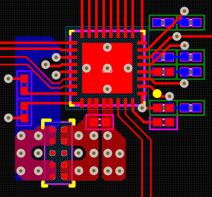
GUID-20220815-SS0I-C2DR-XLWS-SDBSF670X3D4-low.png Figure 9-30 Top Layer GPIO Routing
Table 9-2 Routing Widths
ROUTEWIDTH (MIL MINIMUM)
PA_CC1, PA_CC2, PB_CC1, PB_CC28
VIN_3V3, LDO_3V3, LDO_1V86
Component GND10
GPIO4