JAJSRT9 October 2023 TPS25730
PRODUCTION DATA
- 1
- 1 特長
- 2 アプリケーション
- 3 概要
- 4 Device Comparison Table
- 5 Pin Configuration and Functions
-
6 Specifications
- 6.1 Absolute Maximum Ratings
- 6.2 ESD Ratings
- 6.3 Recommended Operating Conditions
- 6.4 Recommended Capacitance
- 6.5 Thermal Information
- 6.6 Power Supply Characteristics
- 6.7 Power Consumption
- 6.8 PPHV Power Switch Characteristics - TPS25730D
- 6.9 PP_EXT Power Switch Characteristics - TPS25730S
- 6.10 Power Path Supervisory
- 6.11 CC Cable Detection Parameters
- 6.12 CC PHY Parameters
- 6.13 Thermal Shutdown Characteristics
- 6.14 ADC Characteristics
- 6.15 Input/Output (I/O) Characteristics
- 6.16 I2C Requirements and Characteristics
- 6.17 Typical Characteristics
- 7 Parameter Measurement Information
-
8 Detailed Description
- 8.1 Overview
- 8.2 Functional Block Diagram
- 8.3
Feature Description
- 8.3.1 USB-PD Physical Layer
- 8.3.2 Power Management
- 8.3.3 Power Paths
- 8.3.4 Cable Plug and Orientation Detection
- 8.3.5 Overvoltage Protection (CC1, CC2)
- 8.3.6 Default Behavior Configuration (ADCIN1, ADCIN2)
- 8.3.7 ADC
- 8.3.8 Digital Interfaces
- 8.3.9 Digital Core
- 8.3.10 I2C Interface
- 8.3.11 Minimum Voltage Configuration
- 8.3.12 Maximum Voltage Configuration
- 8.3.13 Sink Current Configuration
- 8.3.14 Autonegotiate Sink Minimum Power
- 8.3.15 Extended Sink Capabilities Power Delivery Power
- 8.4 Device Functional Modes
- 8.5 Schottky for Current Surge Protection
- 8.6 Thermal Shutdown
- 9 Application and Implementation
- 10Device and Documentation Support
- 11Revision History
- 12Mechanical, Packaging, and Orderable Information
パッケージ・オプション
メカニカル・データ(パッケージ|ピン)
サーマルパッド・メカニカル・データ
- RSM|32
発注情報
9.4.1.3 Component Placement
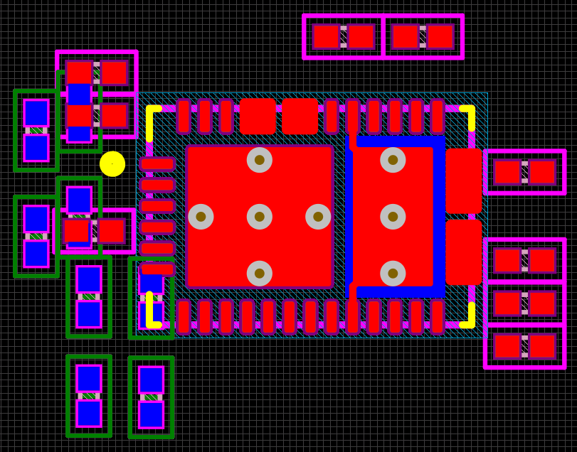
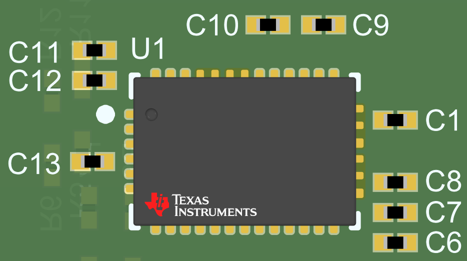
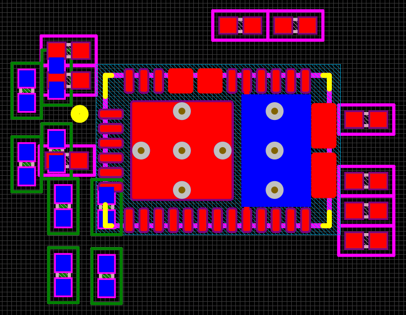
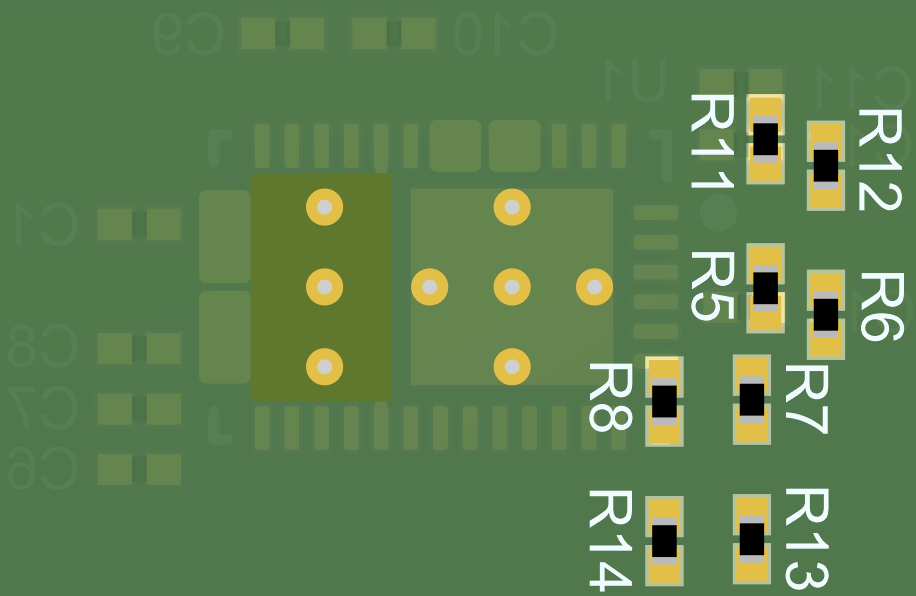
Top and bottom placement is used for this example to minimize solution size. The TPS25730D is placed on the top side of the board and the majority of its components are placed on the bottom side. When placing the components on the bottom side, TI recommends that they are placed directly under the TPS25730D. When placing the VBUS and PPHV capacitors, it is easiest to place them with the GND terminal of the capacitors to face outward from the TPS25730D or to the side because the drain connection pads on the bottom layer must not be connected to anything and left floating. All other components that are for pins on the GND pad side of the TPS25730D must be placed where the GND terminal is underneath the GND pad.
The CC capacitors must be placed on the same side as the TPS25730D close to the respective CC1 and CC2 pins. Do NOT via to another layer in between the CC pins to the CC capacitor, placing a via after the CC capacitor is recommended.
Figure 9-21 through Figure 9-22 show the placement in 2-D and 3-D.
 Figure 9-12 Top View Layout
 Figure 9-14 Top View 3-D
 Figure 9-13 Bottom View Layout
 Figure 9-15 Bottom View 3-D