JAJSJE8A May   2021  – March 2022 TPS25830A-Q1 , TPS25832A-Q1

PRODUCTION DATA  

  1. 特長
  2. アプリケーション
  3. 概要
  4. Revision History
  5. 概要 (続き)
  6. Device Comparison Table
  7. Pin Configuration and Functions
  8. Specifications
    1. 8.1 Absolute Maximum Ratings
    2. 8.2 ESD Ratings
    3. 8.3 Recommended Operating Conditions
    4. 8.4 Thermal Information
    5. 8.5 Electrical Characteristics
    6. 8.6 Timing Requirements
    7. 8.7 Switching Characteristics
    8. 8.8 Typical Characteristics
  9. Parameter Measurement Information
  10. 10Detailed Description
    1. 10.1 Overview
    2. 10.2 Functional Block Diagram
    3. 10.3 Feature Description
      1. 10.3.1  Buck Regulator
      2. 10.3.2  Enable/UVLO and Start-Up
      3. 10.3.3  Switching Frequency and Synchronization (RT/SYNC)
      4. 10.3.4  Spread-Spectrum Operation
      5. 10.3.5  VCC, VCC_UVLO
      6. 10.3.6  Minimum ON-Time, Minimum OFF-Time
      7. 10.3.7  Internal Compensation
      8. 10.3.8  Bootstrap Voltage (BOOT)
      9. 10.3.9  RSNS, RSET, RILIMIT and RIMON
      10. 10.3.10 Overcurrent and Short Circuit Protection
        1. 10.3.10.1 Current Limit Setting using RILIMIT
        2. 10.3.10.2 Current Limit Setting for MFI OCP
        3. 10.3.10.3 Buck Average Current Limit Design Example
        4. 10.3.10.4 External MOSFET Gate Drivers
        5. 10.3.10.5 Cycle-by-Cycle Buck Current Limit
      11. 10.3.11 Overvoltage, IEC and Short to Battery Protection
        1. 10.3.11.1 VBUS and VCSN/OUT Overvoltage Protection
        2. 10.3.11.2 DP_IN and DM_IN Protection
        3. 10.3.11.3 CC IEC and OVP Protection
      12. 10.3.12 Cable Compensation
        1. 10.3.12.1 Cable Compensation Design Example
      13. 10.3.13 USB Port Control
      14. 10.3.14 FAULT Response
      15. 10.3.15 USB Specification Overview
      16. 10.3.16 USB Type-C® Basics
        1. 10.3.16.1 Configuration Channel
        2. 10.3.16.2 Detecting a Connection
        3. 10.3.16.3 Configuration Channel Pins CC1 and CC2
        4. 10.3.16.4 Current Capability Advertisement and VCONN Overload Protection
        5. 10.3.16.5 Plug Polarity Detection
      17. 10.3.17 Device Power Pins (IN, CSN/OUT, and PGND)
      18. 10.3.18 Thermal Shutdown
      19. 10.3.19 Power Wake
    4. 10.4 Device Functional Modes
      1. 10.4.1 Shutdown Mode
      2. 10.4.2 Standby Mode
      3. 10.4.3 Active Mode
      4. 10.4.4 Device Truth Table (TT)
      5. 10.4.5 USB Port Operating Modes
        1. 10.4.5.1 USB Type-C® Mode
        2. 10.4.5.2 Standard Downstream Port (SDP) Mode — USB 2.0, USB 3.0, and USB 3.1
        3. 10.4.5.3 Charging Downstream Port (CDP) Mode
        4. 10.4.5.4 Client Mode
      6. 10.4.6 High-Bandwidth Data-Line Switches
  11. 11Application and Implementation
    1. 11.1 Application Information
    2. 11.2 Typical Application
      1. 11.2.1 Design Requirements
      2. 11.2.2 Detailed Design Procedure
        1. 11.2.2.1  Output Voltage
        2. 11.2.2.2  Switching Frequency
        3. 11.2.2.3  Inductor Selection
        4. 11.2.2.4  Output Capacitor Selection
        5. 11.2.2.5  Input Capacitor Selection
        6. 11.2.2.6  Bootstrap Capacitor Selection
        7. 11.2.2.7  VCC Capacitor Selection
        8. 11.2.2.8  Enable and Undervoltage Lockout Set-Point
        9. 11.2.2.9  Current Limit Set-Point
        10. 11.2.2.10 Cable Compensation Set-Point
        11. 11.2.2.11 LD_DET, POL, and FAULT Resistor Selection
      3. 11.2.3 Application Curves
  12. 12Power Supply Recommendations
  13. 13Layout
    1. 13.1 Layout Guidelines
    2. 13.2 Ground Plane and Thermal Considerations
    3. 13.3 Layout Example
  14. 14Device and Documentation Support
    1. 14.1 Documentation Support
      1. 14.1.1 Related Documentation
    2. 14.2 Related Links
    3. 14.3 ドキュメントの更新通知を受け取る方法
    4. 14.4 サポート・リソース
    5. 14.5 Trademarks
    6. 14.6 静電気放電に関する注意事項
    7. 14.7 用語集
  15. 15Mechanical, Packaging, and Orderable Information

パッケージ・オプション

メカニカル・データ(パッケージ|ピン)
サーマルパッド・メカニカル・データ
発注情報

Typical Characteristics

Unless otherwise specified the following conditions apply: VIN = 13.5 V, fSW = 400 kHz, L = 8.2 µH, COUT_CSP = 66 µF, COUT_CSN = 0.1 µF, CBUS = 1 µF, TA = 25 °C.
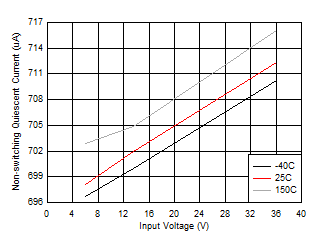
GUID-0B1D0A89-2D9A-480A-B452-39839B3D5372-low.gif
VCSN = 8 VCC1= Rd
Figure 8-1 Non-Switching Quiescent Current
GUID-A3368E16-FD94-4D79-BDAB-669C0D875D5D-low.gif
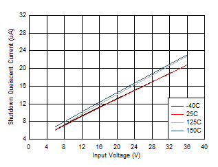
EN = 0 V
Figure 8-3 Shutdown Quiescent Current
GUID-F5D975F2-3A8A-443D-B3B5-6EA53C12DF3E-low.gif
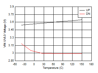
Figure 8-5 VIN UVLO Threshold
GUID-22383E79-8726-4145-80E0-06B4F6EFBF84-low.gif
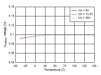
RIMON = 0 Ω
Figure 8-7 VCSN/OUT Voltage vs Junction Temperature
GUID-981F098F-96C7-44F1-84AA-5D0C238F55A4-low.gif
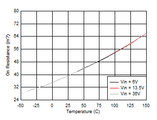
Figure 8-9 High-Side MOSFET on Resistance vs Junction Temperature
GUID-AD3294AE-CC1E-46BB-9754-6F8C03285BC4-low.gif
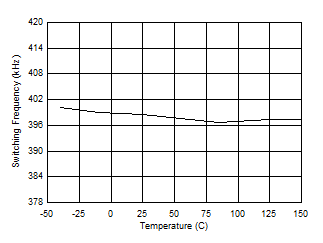
RT = 49.9 kΩ
Figure 8-11 Switching Frequency vs Junction Temperature
GUID-174602AB-C96C-4244-BA66-83A651BDD845-low.gif
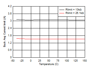
RSNS = 15 mΩ RSET = 300 Ω
Figure 8-13 Buck Average Current Limit vs Junction Temperature
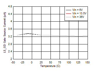
GUID-15BC5FD9-1AFA-47DF-9F96-DC669BA6425D-low.gif
Figure 8-15 LS_GD Gate Source Current vs Junction Temperature
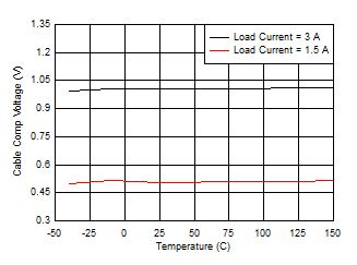
GUID-A685D0F9-8A66-406D-A7E3-4F845A85BCCB-low.gif
RSNS = 15 mΩ RSET = 300 Ω RIMON = 13 kΩ
Figure 8-17 Cable Compensation Voltage vs Junction Temperature
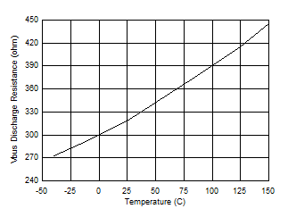
GUID-B3B21960-B81C-4B93-9518-BF69E131F33E-low.gif
Figure 8-19 VBUS Discharge Resistance vs Junction Temperature
GUID-8B8483A9-BEBA-4975-A672-619E5F6F0C06-low.gif
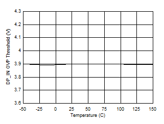
Figure 8-21 DP_IN Overvoltage Protection Threshold vs Junction Temperature
GUID-AFA2A19B-A726-433A-8D57-967706BE46FE-low.gif
VCONN = 5V
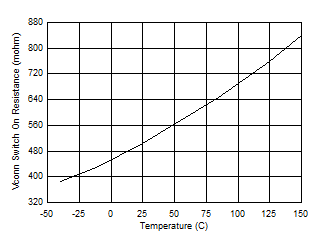
Figure 8-23 VCONN Current Limiting Switch On Resistance vs Junction Temperature
GUID-23757D2F-1FFC-4128-99B2-C6C3881B9C7D-low.gif
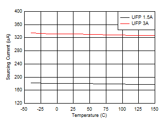
Figure 8-25 CC Sourcing Current vs Junction Temperature
GUID-D643BE8C-5CA2-4300-8567-AC1506D79A7F-low.gif
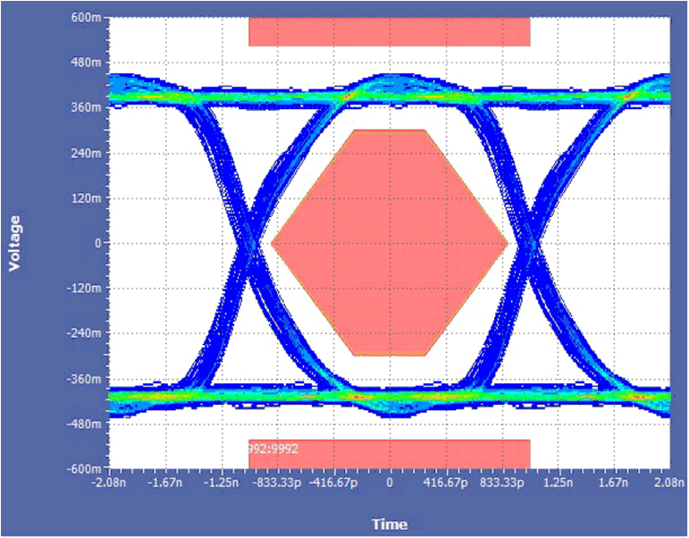
Measured Source with 10-cm cable
Figure 8-27 Bypassing the TPS25830A-Q1 Data Switch
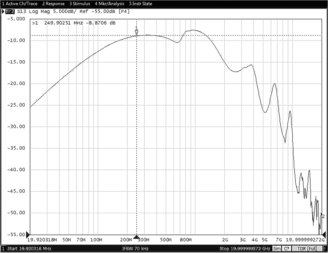
GUID-A541F0B8-8247-4A8E-B13E-9B716BFDA67B-low.gif
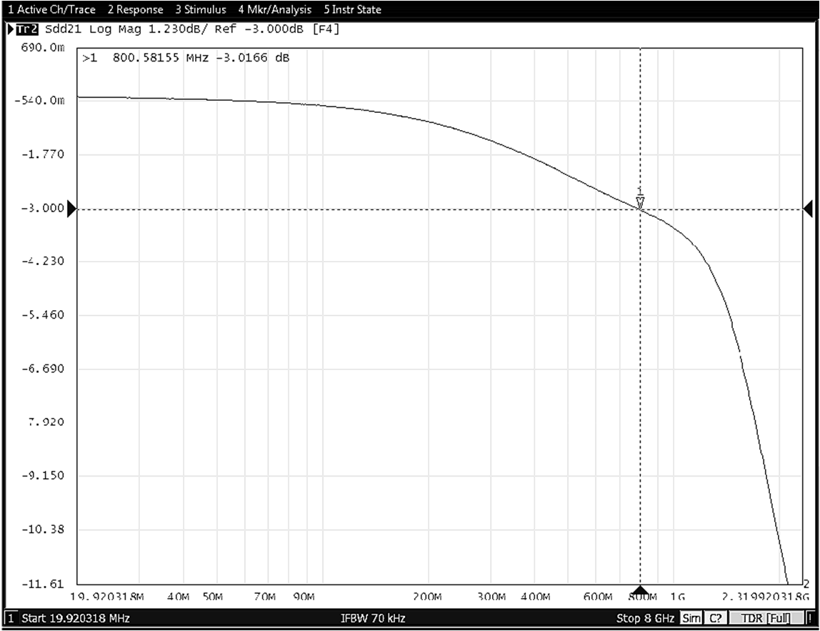
Figure 8-29 Data Transmission Characteristics vs Frequency (TPS25830A-Q1)
GUID-E573F364-D3E3-406F-9106-531B31BF6EBC-low.gif
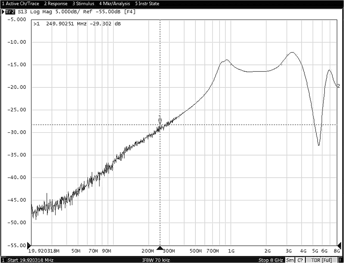
Figure 8-31 On-State Cross-Channel Isolation vs Frequency (TPS25830A-Q1)
GUID-E761FC20-A59B-4F8F-9338-FB5457890A6E-low.gif
CC1 = OPENCC2 = OPEN
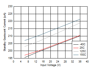
Figure 8-2 Standby Quiescent Current
GUID-D2382816-EE45-4125-A1BE-B039E993543D-low.gif
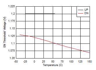
Figure 8-4 Precision Enable Threshold
GUID-BBAB13D6-4A05-4F1C-A375-4EE90C9F75D7-low.gif
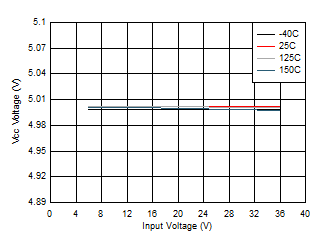
Figure 8-6 VCC vs Input Voltage
GUID-20210513-CA0I-HPFW-TRVQ-TPXHSD6L4TVG-low.svg
Figure 8-8 High-Side Current Limit vs Input Voltage
GUID-C43163C0-129B-4A92-888B-099264CE84E6-low.gif
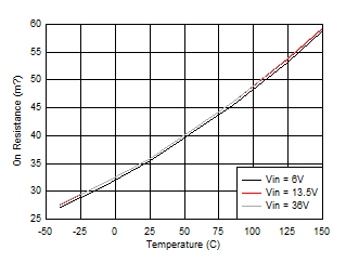
Figure 8-10 Low-Side MOSFET on Resistance vs Junction Temperature
GUID-37957757-AB6B-4C0B-AE72-F28999BC7FC3-low.gif
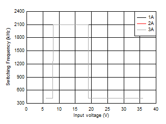
RT = 8.66 kΩ
Figure 8-12 Switching Frequency vs VIN Voltage
GUID-EFC5080C-E75C-4F8C-8D27-0AF17E2FAEA6-low.gif
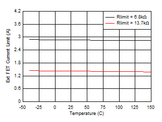
RSNS = 15 mΩ RSET = 300 Ω
Figure 8-14 External FET Current Limit vs Junction Temperature
GUID-BF8A7F71-651F-4B51-93B7-2DF8C80755DF-low.gif
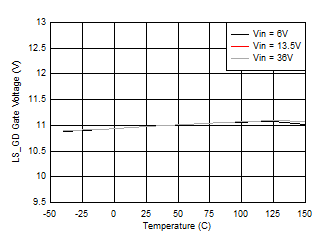
VCSN/OUT = 5.1 V RIMON = 0 kΩ
Figure 8-16 LS_GD Gate Voltage vs Junction Temperature
GUID-DB3C33BE-A860-4393-BE05-1AFF09EC35BB-low.gif
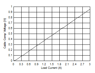
RSNS = 15 mΩ RSET = 300 Ω RIMON = 13 kΩ
Figure 8-18 Cable Compensation Voltage vs Load Current
GUID-641D1145-8BE4-47FB-AF8B-5AC5B3D5CBC4-low.gif
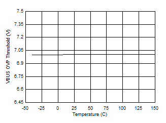
Figure 8-20 VBUS Overvoltage Protection Threshold vs Junction Temperature
GUID-E59E201D-CFB0-418A-B920-417A889EBD27-low.gif
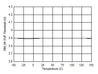
Figure 8-22 DM_IN Overvoltage Protection Threshold vs Junction Temperature
GUID-0441A934-F9CE-47C9-843A-5DF22B72360B-low.gif
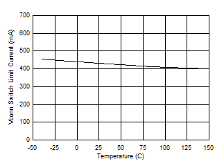
VCONN = 5 V
Figure 8-24 VCONN Switch Current Limit vs Junction Temperature
GUID-4154DE23-B9E2-4FE6-A37F-2A62C8987E34-low.gif
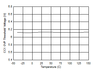
Figure 8-26 CC1 Overvoltage Protection Threshold vs Junction Temperature
GUID-E7DA0577-59E2-4646-B443-5DC37F8E1FC4-low.gif
Measured on TPS25830-Q1 EVM with 10-cm cable
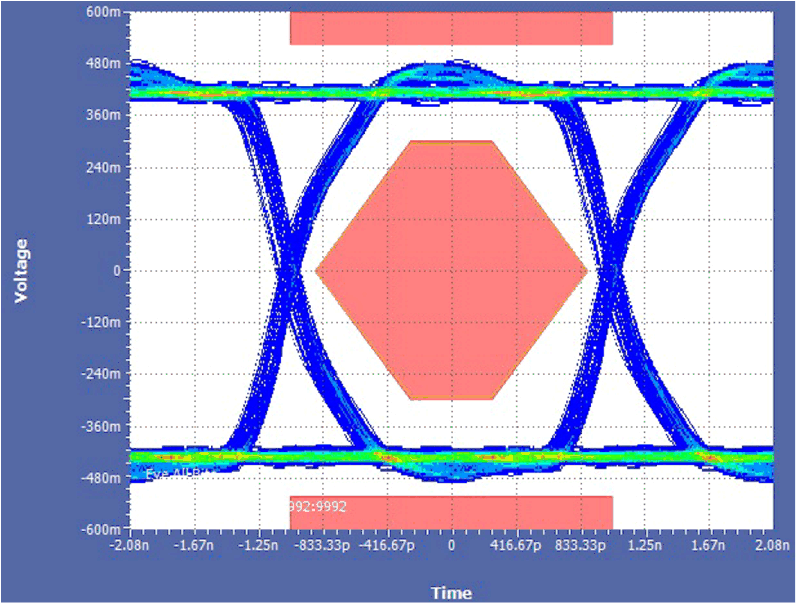
Figure 8-28 Through the TPS25830A-Q1 Data Switch
GUID-33085B4E-1F62-4BAC-BA75-5FB3C92E57E2-low.gif
Figure 8-30 Off-State Data-Switch Isolation vs Frequency (TPS25830A-Q1)