JAJSHY1E September 2019 – March 2022 TPS25840-Q1 , TPS25842-Q1
PRODUCTION DATA
- 1 特長
- 2 アプリケーション
- 3 概要
- 4 Revision History
- 5 概要 (続き)
- 6 Device Comparison Table
- 7 Pin Configuration and Functions
- 8 Specifications
- 9 Parameter Measurement Information
-
10Detailed Description
- 10.1 Overview
- 10.2 Functional Block Diagram
- 10.3
Feature Description
- 10.3.1 Buck Regulator
- 10.3.2 Enable/UVLO
- 10.3.3 Switching Frequency and Synchronization (RT/SYNC)
- 10.3.4 Spread-Spectrum Operation
- 10.3.5 VCC, VCC_UVLO
- 10.3.6 Minimum ON-time, Minimum OFF-time
- 10.3.7 Internal Compensation
- 10.3.8 Bootstrap Voltage (BOOT)
- 10.3.9 RSNS, RSET, RILIMIT and RIMON
- 10.3.10 Overcurrent and Short Circuit Protection
- 10.3.11 Overvoltage, IEC and Short-to-Battery Protection
- 10.3.12 Cable Compensation
- 10.3.13 USB Port Control
- 10.3.14 FAULT Response
- 10.3.15 USB Specification Overview
- 10.3.16 Device Power Pins (IN, CSN/OUT, and PGND)
- 10.3.17 Thermal Shutdown
- 10.4 Device Functional Modes
-
11Application and Implementation
- 11.1 Application Information
- 11.2
Typical Application
- 11.2.1 Design Requirements
- 11.2.2
Detailed Design Procedure
- 11.2.2.1 Output Voltage
- 11.2.2.2 Switching Frequency
- 11.2.2.3 Inductor Selection
- 11.2.2.4 Output Capacitor Selection
- 11.2.2.5 Input Capacitor Selection
- 11.2.2.6 Bootstrap Capacitor Selection
- 11.2.2.7 VCC Capacitor Selection
- 11.2.2.8 Enable and Under Voltage Lockout Set-Point
- 11.2.2.9 Current Limit Set-Point
- 11.2.2.10 Cable Compensation Set-Point
- 11.2.2.11 FAULT Resistor Selection
- 11.2.3 Application Curves
- 12Power Supply Recommendations
- 13Layout
- 14Device and Documentation Support
- 15Mechanical, Packaging, and Orderable Information
パッケージ・オプション
メカニカル・データ(パッケージ|ピン)
- RHB|32
サーマルパッド・メカニカル・データ
- RHB|32
発注情報
10.3.3 Switching Frequency and Synchronization (RT/SYNC)
The switching frequency of the TPS2584x-Q1 can be programmed by the resistor RT from the RT/SYNC pin and GND pin. Use Equation 3 to determine the RT resistance for a given switching frequency.

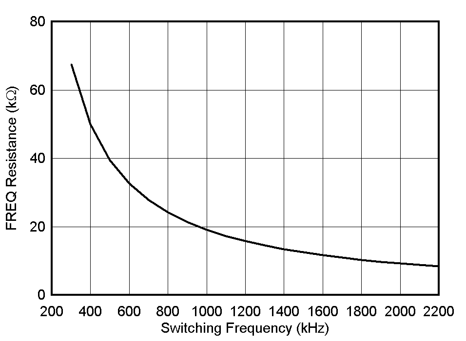 Figure 10-6 RT Set Resistor vs Switching Frequency
Table 10-1 lists typical RT resistors values.
| RT (kΩ) | SWITCHING FREQUENCY (kHz) |
|---|---|
| 68.1 | 300 |
| 49.9 | 400 |
| 39.2 | 500 |
| 19.1 | 1000 |
| 12.4 | 1500 |
| 9.31 | 2000 |
| 8.87 | 2100 |
| 8.45 | 2200 |
TPS2584x-Q1 switching action can be synchronized to an external clock from 300 kHz to 2.3 MHz. The RT/SYNC pin can be used to synchronize the internal oscillator to an external clock. The internal oscillator can be synchronized by AC coupling a positive edge into the RT/SYNC pin. The AC coupled peak-to-peak voltage at the RT/SYNC pin must exceed the SYNC amplitude threshold of 3.5 V (typical) to trip the internal synchronization pulse detector, and the minimum SYNC clock ON and OFF time must be longer than 100 ns (typical). When using a low impedance signal source, the frequency setting resistor, RT, is connected in parallel with an AC coupling capacitor, CCOUP, to a termination resistor, RTERM (for example: 50 Ω). The two resistors in series provide the default frequency setting resistance when the signal source is turned off. A 10-pF ceramic capacitor can be used for CCOUP. Figure 10-7 show the device synchronized to an external clock.
 Figure 10-7 Synchronize to External Clock
To avoid AM radio frequency brand and maintain proper regulation when minimum ON-time or minimum OFF-time is reached, the TPS2584x-Q1 implement frequency foldback scheme depends on VIN voltage. Refer to Figure 8-10.
- When 8 V < VIN ≤ 19 V, the switching frequency of TPS2584x-Q1 is determined by RT resistor or external sync clock.
- When VIN ≤ 8 V, the switching frequency of TPS2584x-Q1 is set to default 420 kHz, regardless of RT resistor setting or external sync clock.
- When VIN > 19 V, the switching frequency of TPS2584x-Q1 is set to default 420 kHz, regardless of RT resistor setting or external sync clock.
figure 10-8, figure 10-9 and Figure 10-10 show the device switching frequency and behavior under different VIN voltage and RT = 8.87 kΩ.
Figure 10-11, Figure 10-12 and Figure 10-13 show the device switching frequency and behavior under different VIN voltage and synchronized to an external 2.1-M system clock.
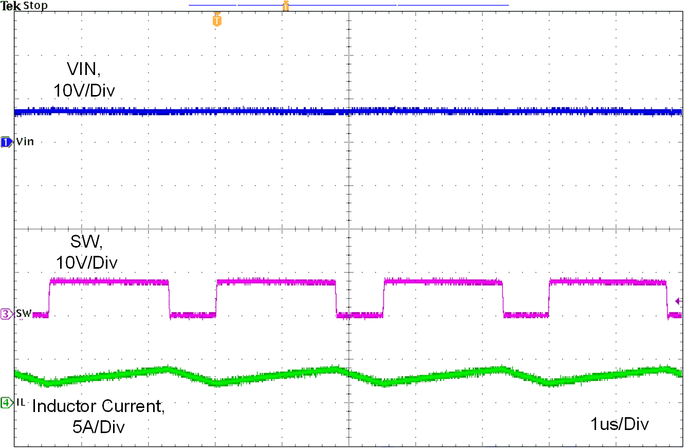
| VIN = 7.5 V | L = 2.2 uH | ILOAD = 3 A |
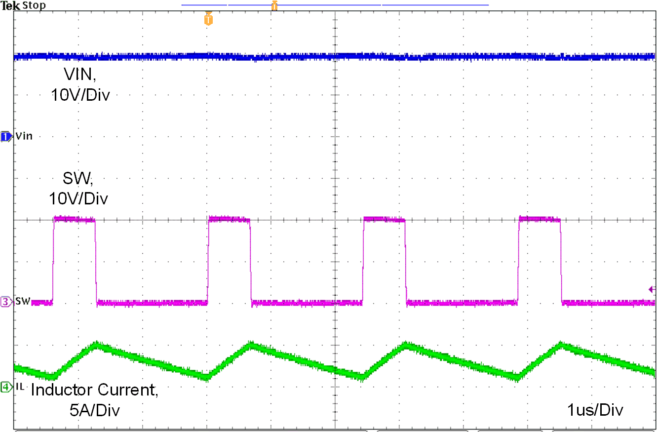
| VIN = 20 V | L = 2.2 uH | ILOAD = 3 A |
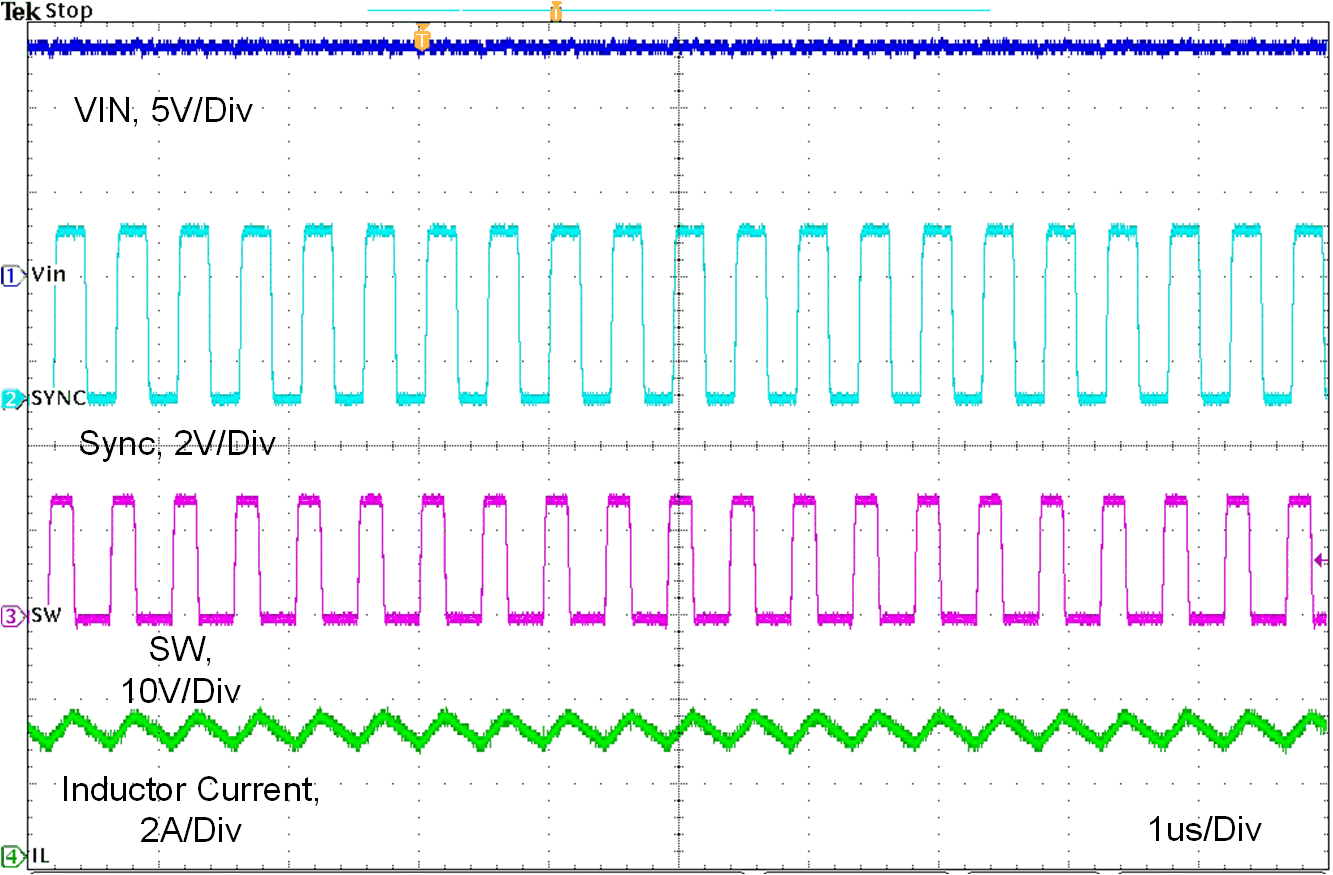
| VIN = 13.5 V | L = 2.2 uH | ILOAD = 3 A |
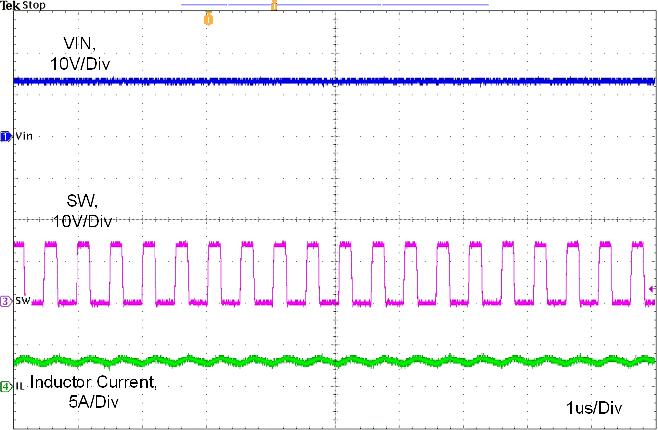
| VIN = 13.5 V | L = 2.2 uH | ILOAD = 3 A |
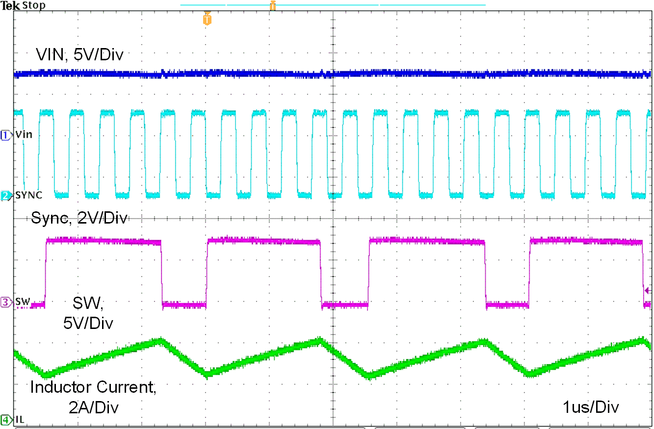
| VIN = 7.5 V | L = 2.2 uH | ILOAD = 3 A |
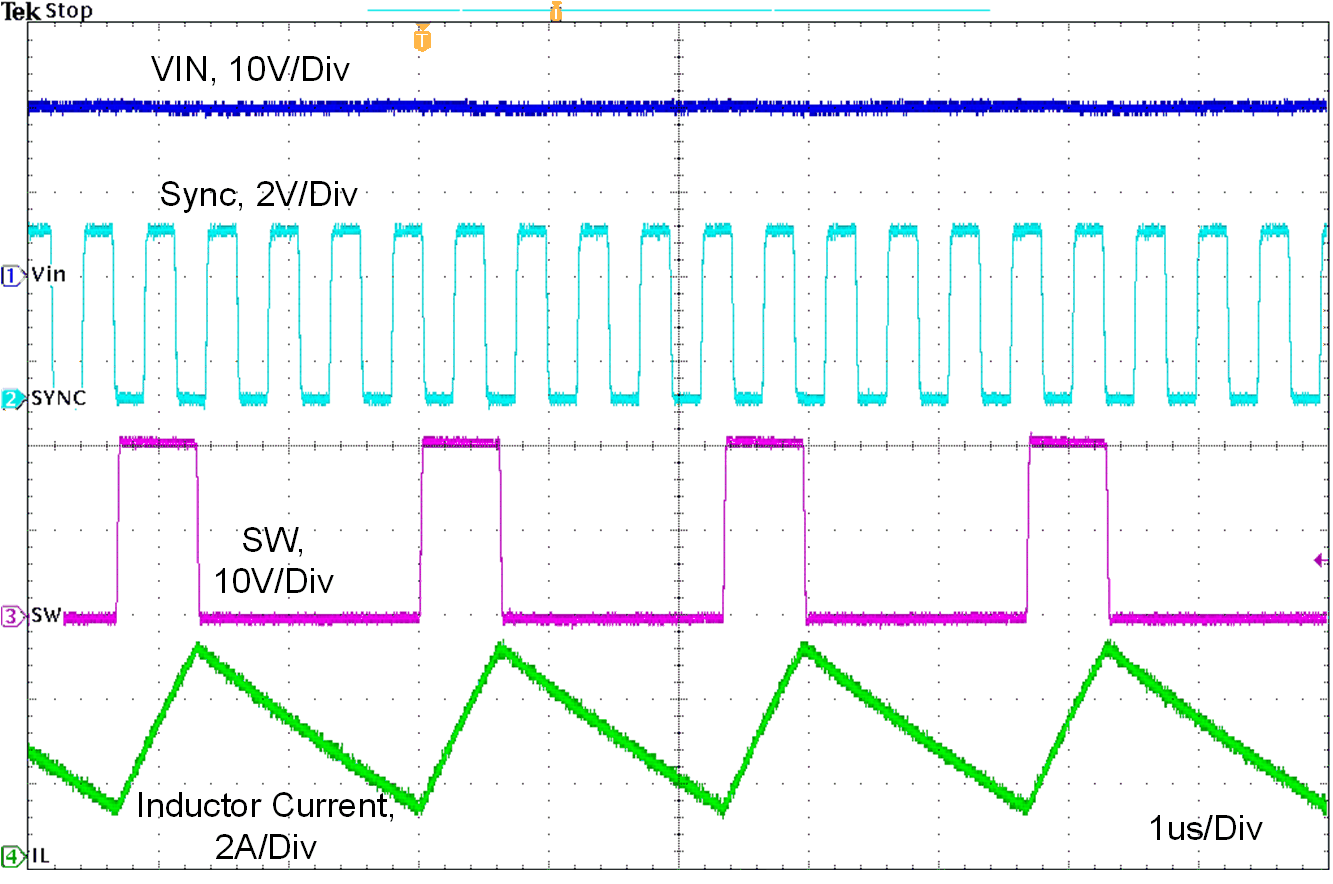
| VIN = 20 V | L = 2.2 uH | ILOAD = 3 A |