JAJSN20 September 2021 TPS25854-Q1 , TPS25855-Q1
PRODUCTION DATA
- 1 特長
- 2 アプリケーション
- 3 概要
- 4 Revision History
- 5 概要 (続き)
- 6 Device Comparison Table
- 7 Pin Configuration and Functions
- 8 Specifications
- 9 Parameter Measurement Information
-
10Detailed Description
- 10.1 Overview
- 10.2 Functional Block Diagram
- 10.3
Feature Description
- 10.3.1 Power Down or Undervoltage Lockout
- 10.3.2 Input Overvoltage Protection (OVP) - Continuously Monitored
- 10.3.3 Buck Converter
- 10.3.4 FREQ/SYNC
- 10.3.5 Bootstrap Voltage (BOOT)
- 10.3.6 Minimum ON-time, Minimum OFF-time
- 10.3.7 Internal Compensation
- 10.3.8 Current Limit and Short Circuit Protection
- 10.3.9 Cable Compensation
- 10.3.10 Thermal Management With Temperature Sensing (TS) and OTSD
- 10.3.11 Thermal Shutdown
- 10.3.12 FAULT Indication
- 10.3.13 USB Specification Overview
- 10.3.14 USB Type-C® Basics
- 10.3.15 USB Port Operating Modes
- 10.4 Device Functional Modes
-
11Application and Implementation
- 11.1 Application Information
- 11.2
Typical Applications
- 11.2.1 Design Requirements
- 11.2.2
Detailed Design Procedure
- 11.2.2.1 Output Voltage Setting
- 11.2.2.2 Switching Frequency
- 11.2.2.3 Inductor Selection
- 11.2.2.4 Output Capacitor Selection
- 11.2.2.5 Input Capacitor Selection
- 11.2.2.6 Bootstrap Capacitor Selection
- 11.2.2.7 Undervoltage Lockout Set-Point
- 11.2.2.8 Cable Compensation Set-Point
- 11.2.2.9 FAULT, POL, and THERM_WARN Resistor Selection
- 11.2.3 Application Curves
- 12Power Supply Recommendations
- 13Layout
- 14Device and Documentation Support
- 15Mechanical, Packaging, and Orderable Information
10.3.1 Power Down or Undervoltage Lockout
The device is in power down mode if the IN terminal voltage is less than VUVLO. The part is considered dead and all the terminals are high impedance. Once the IN voltage rises above the VUVLO threshold, the IC enters sleep mode or active mode depending on the EN/UVLO voltage.
The voltage on the EN/UVLO pin controls the ON/OFF operation of TPS2585x-Q1. An EN/UVLO pin voltage higher than VEN/UVLO-H is required to start the internal regulator and begin monitoring the CCn lines for a valid Type-C connection. The internal USB monitoring circuitry is on when VIN is within the operation range and the EN/UVLO threshold is cleared. The buck regulator starts to operate, however, the USB ports load switch remain OFF until a valid Type-C detection has been made. This feature ensures the cold socket (0 V) USB Type-C VBUS requirement is met.
The EN/UVLO pin is an input and cannot be left open or floating. The simplest way to enable the operation of the TPS2585x-Q1 is to connect the EN to SENSE. This connection allows self-start-up of the TPS2585x-Q1 when VIN is within the operation range. Note that cannot connect the EN to IN pin directly for self-start-up.
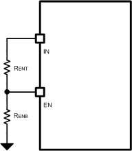
Many applications benefit from the employment of an enable divider RENT and RENB to establish a precision system UVLO level for the TPS2585x-Q1, shown in Figure 10-1. The system UVLO can be used for sequencing, ensuring reliable operation, or supply protection, such as a battery discharge level. To ensure the USB ports VBUS is within the 5-V operating range as required for USB compliance (for the latest USB specifications and requirements, refer to USB.org), TI suggests that the RENT and RENB resistors be chosen such that the TPS2585x-Q1 enables when VIN is approximately 6 V. Considering the drop out voltage of the buck regulator and IR loses in the system, 6 V provides adequate margin to maintain VBUS within USB specifications. If system requirements such as a warm crank (start) automotive scenario require operation with VIN < 6 V, the values of RENT and RENB can be calculated assuming a lower VIN. An external logic signal can also be used to drive EN/UVLO input when a microcontroller is present and it is desirable to enable or disable the USB port remotely for other reasons.
 Figure 10-1 System UVLO by Enable Divider
UVLO configuration using external resistors is governed by the following equations:


Example:
VIN(ON) = 6V
RENT = 20 kΩ
RENB = 5 kΩ
Therefore VIN(OFF) = 5.5 V