JAJSHD7 May 2019 TPS2596
ADVANCE INFORMATION for pre-production products; subject to change without notice.
- 1 特長
- 2 アプリケーション
- 3 概要
- 4 改訂履歴
- 5 デバイス比較表
- 6 Pin Configuration and Functions
- 7 Specifications
-
8 Detailed Description
- 8.1 Overview
- 8.2 Feature Description
- 8.3 Functional Block Diagram
- 8.4 Feature Description
- 8.5 Device Functional Modes
-
9 Application and Implementation
- 9.1 Application Information
- 9.2
Typical Application
- 9.2.1 Precision Current Limiting and Protection for White Goods
- 9.2.2 Design Requirements
- 9.2.3 Detailed Design Procedure
- 9.2.4 Support Component Selection: RFLT and CIN
- 9.2.5 Application Curves
- 9.3 System Examples
- 10Power Supply Recommendations
- 11Layout
- 12デバイスおよびドキュメントのサポート
- 13メカニカル、パッケージ、および注文情報
パッケージ・オプション
メカニカル・データ(パッケージ|ピン)
- DDA|8
サーマルパッド・メカニカル・データ
- DDA|8
発注情報
7.7 Switching Characteristics
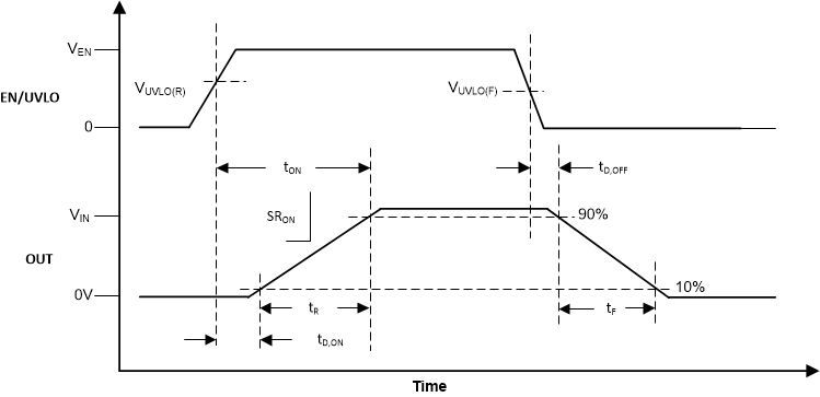
The output rising slew rate is internally controlled and constant across the entire operating voltage range to ensure the turn on timing is not affected by the load conditions. The rising slew rate can be adjusted by adding capacitance from the dVdt pin to ground. As CdVdt is increased it will slow the rising slew rate (SR). See Slew Rate and Inrush Current Control (dVdt) section for more details. The fall time, however, is dependent on the RC time constant of the load capacitance (COUT) and Load Resistance (RL). The Switching Characteristics are only valid for the power-up sequence where the supply is available in steady state condition and the load voltage is completely discharged before the device is enabled.Typical Values are taken at TJ = 25°C unless specifically noted otherwise. ROUT = 100 Ω, COUT = 1 µF| PARAMETER | VIN
|
CdVdt = Open | CdVdt = 3300pF | UNIT | |
|---|---|---|---|---|---|
| SRON | Output Rising slew rate | 2.7 V | 28.9 | 11.0 | V/ms |
| 5 V | 42.7 | 12 | |||
| 12 V | 75.1 | 12.9 | |||
| tD,ON | Turn on delay | 2.7 V | 77.5 | 241.1 | µs |
| 5 V | 78.9 | 269.8 | |||
| 12 V | 82.9 | 337.9 | |||
| tR | Rise time | 2.7 V | 74.7 | 196.9 | µs |
| 5 V | 94.1 | 333.8 | |||
| 12 V | 128.4 | 747 | |||
| tON | Turn on time | 2.7 V | 152.2 | 438 | µs |
| 5 V | 173 | 603.6 | |||
| 12 V | 211.3 | 1084.9 | |||
| tD,OFF | Turn off delay | 2.7 V | 12.2 | 12.3 | µs |
| 5 V | 11.6 | 11.9 | |||
| 12 V | 10.3 | 10.4 | |||
 Figure 1. TPS2596xx Switching Times