JAJSHD7 May   2019 TPS2596

ADVANCE INFORMATION for pre-production products; subject to change without notice.  

  1. 特長
  2. アプリケーション
  3. 概要
    1.     Device Images
      1.      概略回路図
      2.      TPS25963x の 1kV EFT 応答
  4. 改訂履歴
  5. デバイス比較表
  6. Pin Configuration and Functions
    1. Table 1. Pin Functions
  7. Specifications
    1. 7.1 Absolute Maximum Ratings
    2. 7.2 ESD Ratings
    3. 7.3 Recommended Operating Conditions
    4. 7.4 Thermal Information
    5. 7.5 Electrical Characteristics
    6. 7.6 Timing Requirements
    7. 7.7 Switching Characteristics
    8. 7.8 Typical Characteristics
  8. Detailed Description
    1. 8.1 Overview
    2. 8.2 Feature Description
    3. 8.3 Functional Block Diagram
      1. 8.3.1 TPS25962x Block Diagram
      2. 8.3.2 TPS25963x Block Diagram
    4. 8.4 Feature Description
      1. 8.4.1 Undervoltage Protection (UVP) and Undervoltage Lockout (UVLO)
      2. 8.4.2 Overvoltage Protection
        1. 8.4.2.1 Overvoltage Lockout
        2. 8.4.2.2 Overvoltage Clamp
      3. 8.4.3 Inrush Current, Overcurrent and Short Circuit Protection
        1. 8.4.3.1 Slew Rate and Inrush Current Control (dVdt)
        2. 8.4.3.2 Active Current Limiting
        3. 8.4.3.3 Short Circuit Protection
      4. 8.4.4 Analog Load Current Monitor (IMON)
      5. 8.4.5 Overtemperature Protection (OTP)
      6. 8.4.6 Fault Indication
    5. 8.5 Device Functional Modes
      1. 8.5.1 Enable and Fault Pin Functional Mode 1: Single Device, Self-Controlled
      2. 8.5.2 Enable and Fault Pin Functional Mode 2: Single Device, Host-Controlled
      3. 8.5.3 Enable and Fault Pin Functional Mode 3: Multiple Devices, Self-Controlled
  9. Application and Implementation
    1. 9.1 Application Information
    2. 9.2 Typical Application
      1. 9.2.1 Precision Current Limiting and Protection for White Goods
      2. 9.2.2 Design Requirements
      3. 9.2.3 Detailed Design Procedure
        1. 9.2.3.1 Programming the Current-Limit Threshold: RILM Selection
        2. 9.2.3.2 Undervoltage and Overvoltage Lockout Set Point
        3. 9.2.3.3 Setting Output Voltage Ramp Time (TdVdT)
          1. 9.2.3.3.1 Case 1: Start-Up Without Load. Only Output Capacitance COUT Draws Current
          2. 9.2.3.3.2 Case 2: Start-Up With Load. Output Capacitance COUT and Load Draw Current
      4. 9.2.4 Support Component Selection: RFLT and CIN
      5. 9.2.5 Application Curves
    3. 9.3 System Examples
      1. 9.3.1 Current Limiting and Overvoltage Protection and for Energy Meter Power Rails
      2. 9.3.2 Precision Current Limiting and Protection in Appliances
  10. 10Power Supply Recommendations
    1. 10.1 Transient Protection
    2. 10.2 Output Short-Circuit Measurements
  11. 11Layout
    1. 11.1 Layout Guidelines
    2. 11.2 Layout Example
  12. 12デバイスおよびドキュメントのサポート
    1. 12.1 ドキュメントのサポート
      1. 12.1.1 関連資料
    2. 12.2 ドキュメントの更新通知を受け取る方法
    3. 12.3 コミュニティ・リソース
    4. 12.4 商標
    5. 12.5 静電気放電に関する注意事項
    6. 12.6 Glossary
  13. 13メカニカル、パッケージ、および注文情報

パッケージ・オプション

メカニカル・データ(パッケージ|ピン)
サーマルパッド・メカニカル・データ
発注情報

Typical Characteristics

TPS2596 Waveform-Hotplug.png
VIN = 12 V, COUT = 220 μF, RILM = 453 Ω
Figure 2. Input Hotplug Response
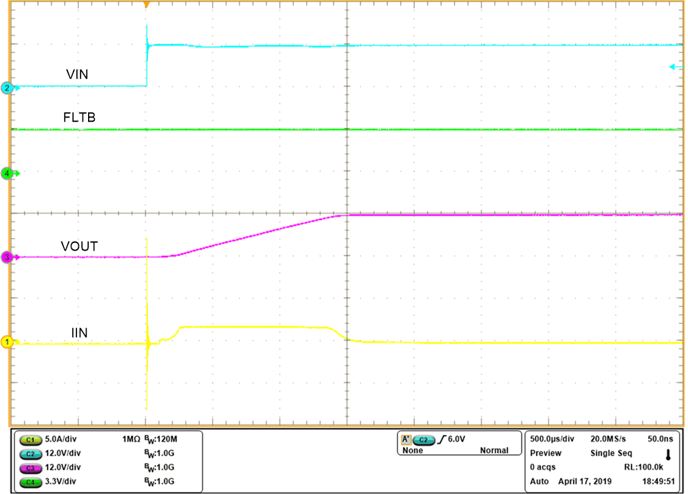
TPS2596 Waveform-Inrush-dVdt-limited.png
VIN = 12 V, COUT = 10 μF, RILM = 453 Ω, CDVDT = 2200 pF
Figure 3. Output Voltage Ramp and Inrush Current at Start Up, CdVdT = 2200 pF
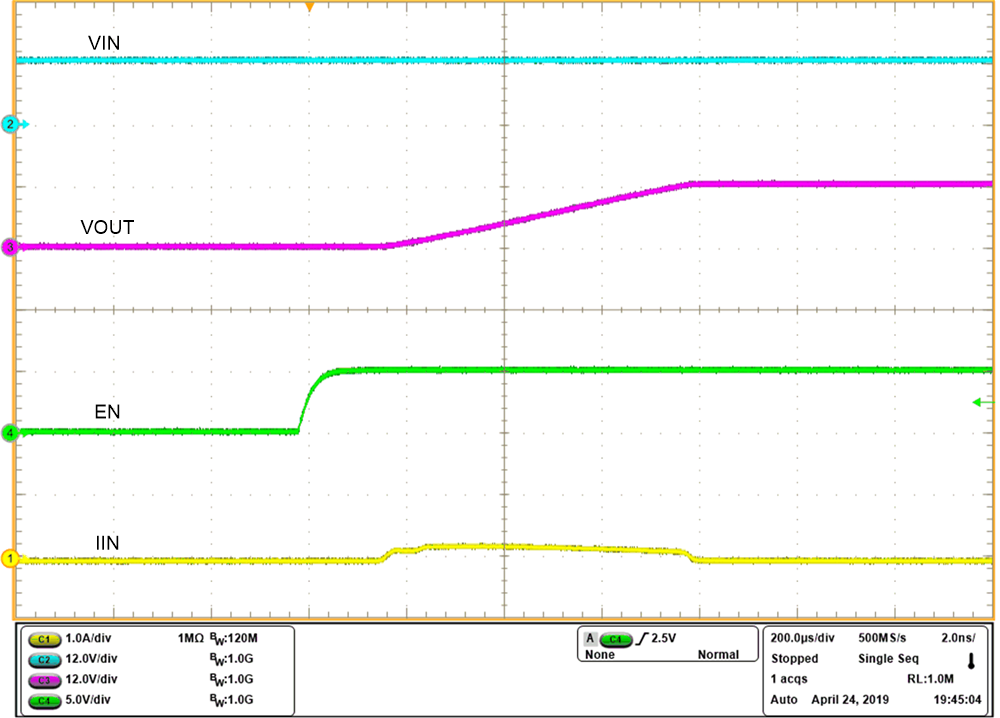
TPS2596 Waveform-Inrush-no-dVdt-control.png
VIN = 12 V, COUT = 10 μF, RILM = 453 Ω, CDVDT = OPEN
Figure 4. Output Voltage Ramp and Inrush Current at Start Up, CdVdT = OPEN
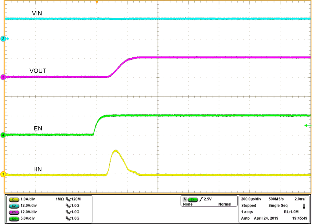
TPS2596 Waveform-Wake-up-with-EN.png
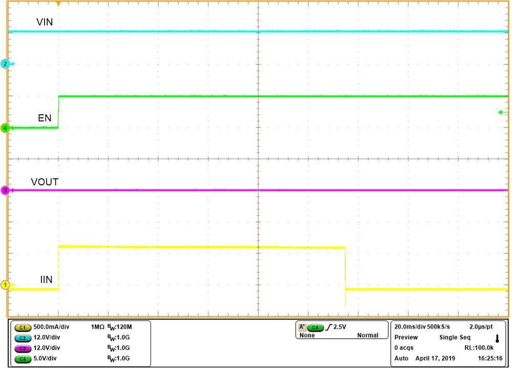
VIN = 12 V, VEN = 3.3 V
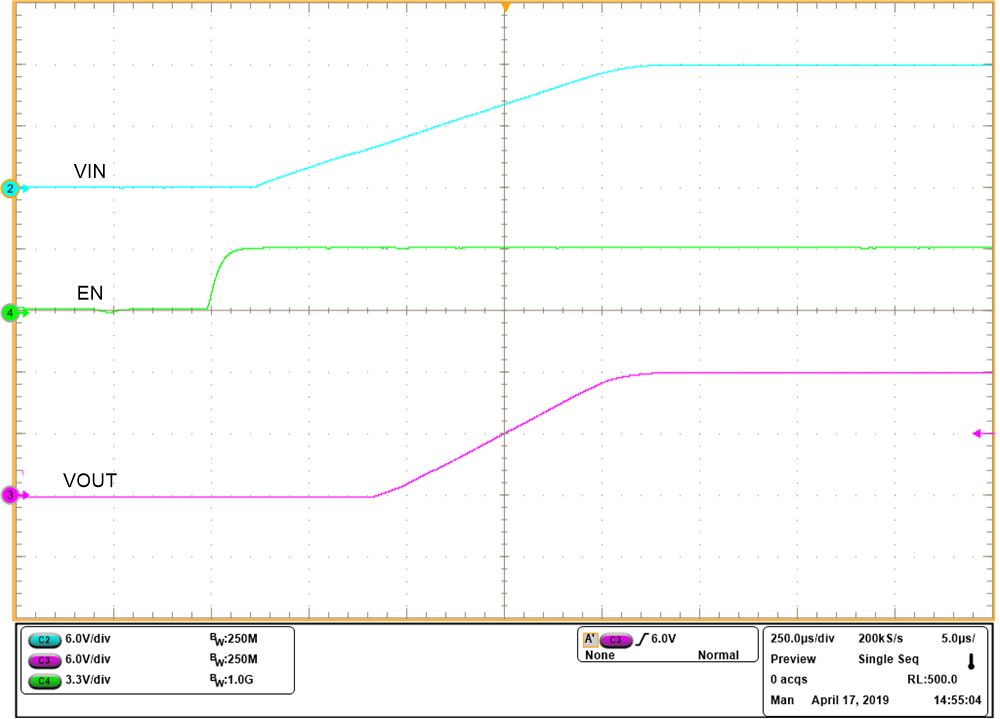
Figure 5. Turn ON with EN
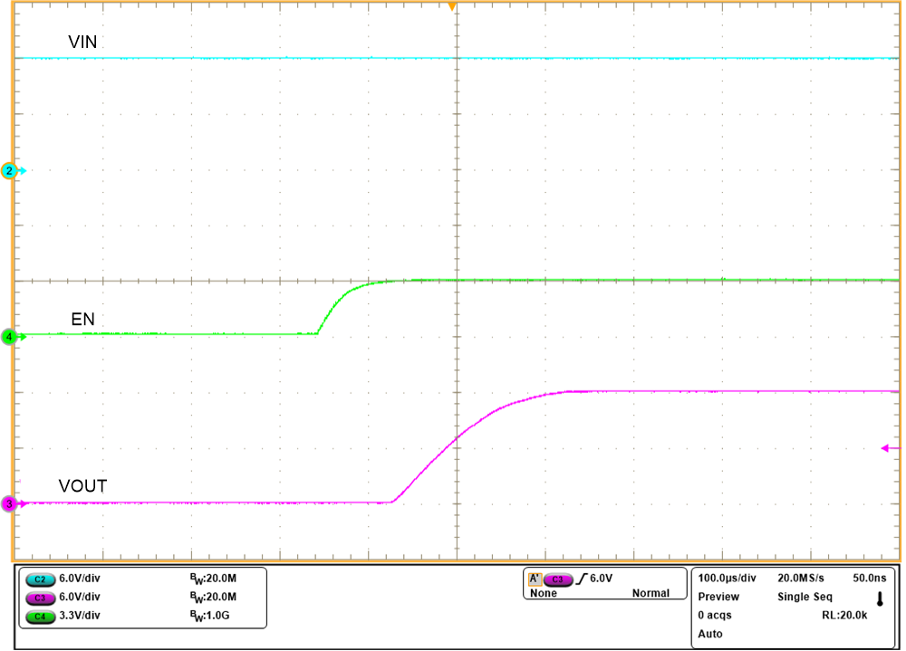
TPS2596 Waveform-Wake-up-with-VIN.png
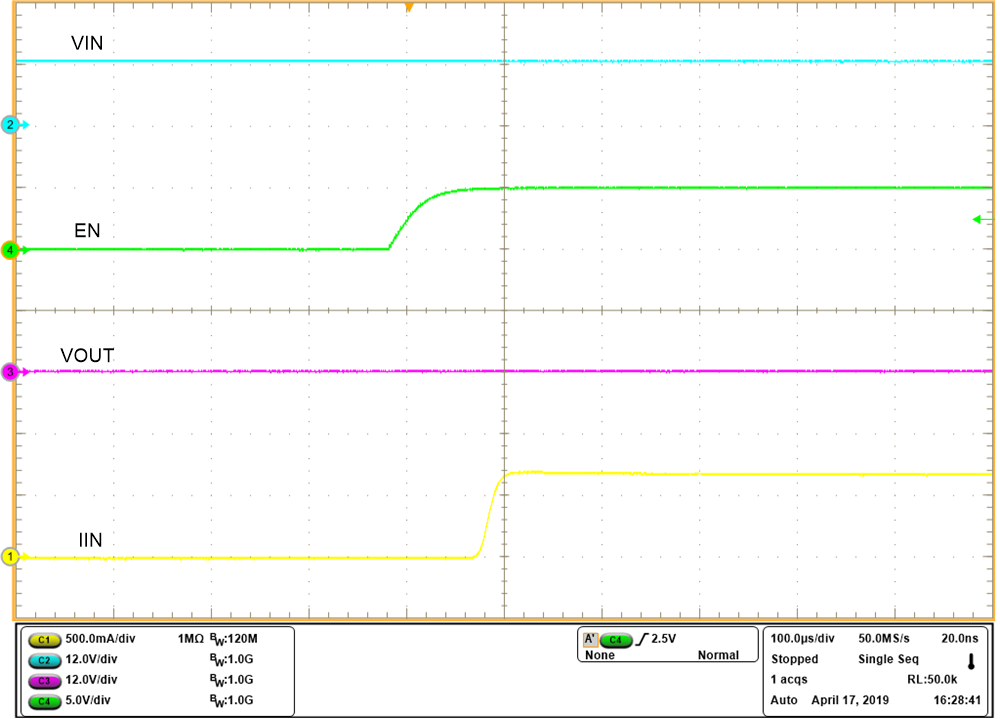
VIN = 12 V, VEN = 3.3 V
Figure 6. Turn ON with VIN
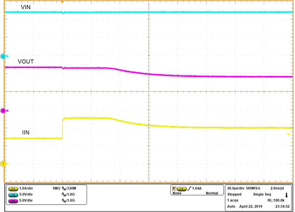
TPS2596 Waveform-CL-Load-Step.png
VIN = 12 V, RILM = 453 Ω, ROUT Varied From 8.33 Ω to 4.54 Ω
Figure 7. Overcurrent Response
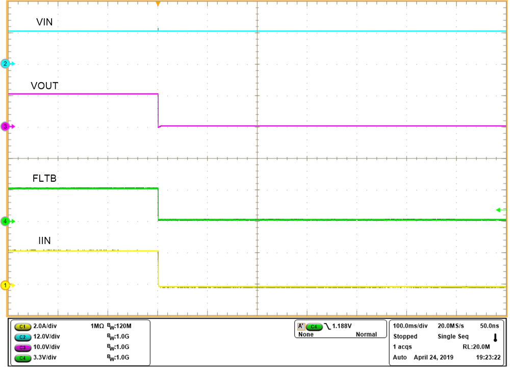
TPS2596 Waveform-CL-TSD-Latch-off.png
VIN = 12 V, RILM = 453 Ω, ROUT = 5 Ω
Figure 8. Thermal Shutdown Latch-off Response - TPS2596x0
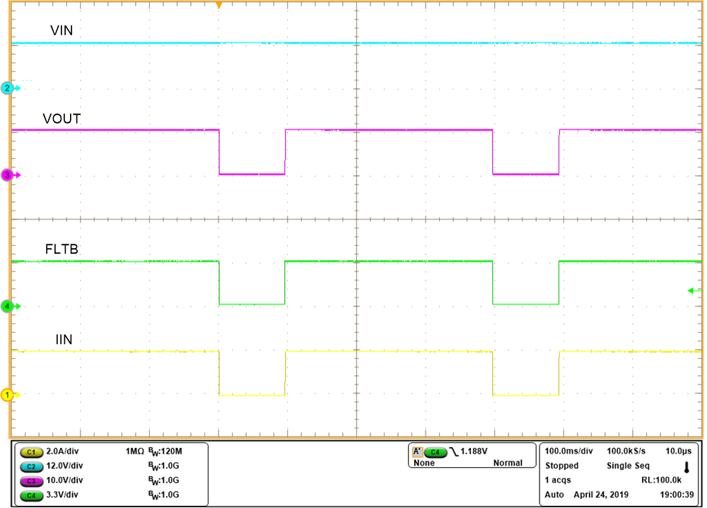
TPS2596 Waveform-CL-TSD-Auto-retry.png
VIN = 12 V, RILM = 453 Ω, ROUT = 5 Ω
Figure 9. Thermal Shutdown Auto-Retry Response - TPS2596x1
TPS2596 Waveform-Hotshort-while-ON.png
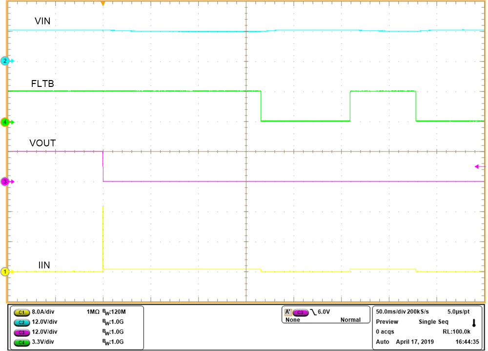
VIN = 12 V, RILM = 453 Ω
Figure 10. Short-Circuit While ON Response
TPS2596 Waveform-Hotshort-while-ON-zoomed.png
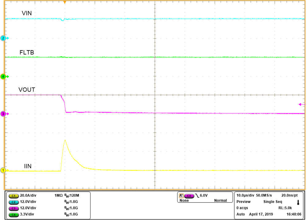
VIN = 12 V, RILM = 453 Ω
Figure 11. Short-Circuit While ON Response (Zoomed In)
TPS2596 Waveform-Power-up-into-short.png
VIN = 12 V, RILM = 453 Ω
Figure 12. Power Up Into Short-Circuit
TPS2596 Waveform-Power-up-into-short-zoomed.png
VIN = 12 V, RILM = 453 Ω
Figure 13. Power Up Into Short-Circuit (Zoomed In)
TPS2596 Waveform-OVLO-entry.png
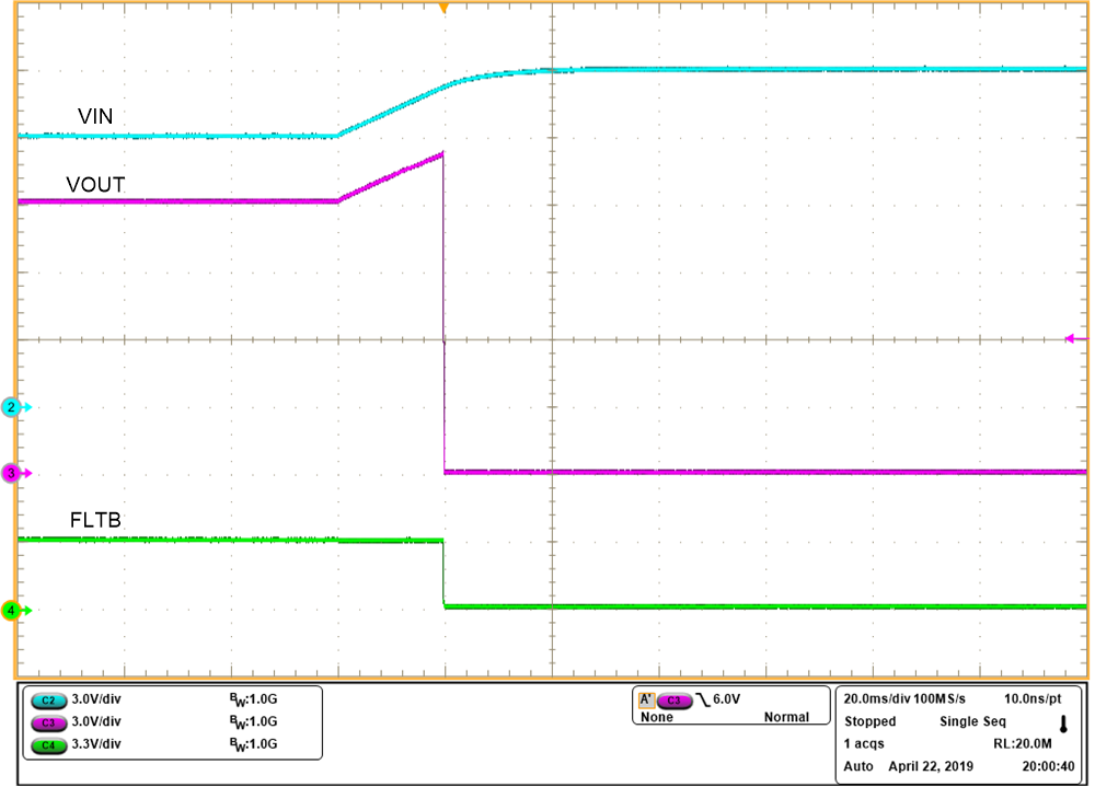
VIN increased from 12 V to 15 V
Figure 14. TPS25963x Overvoltage Lockout Response
TPS2596 Waveform-OVC-3-7V.png
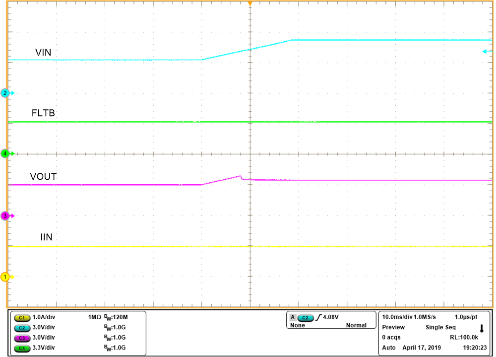
OVCSEL = Shorted to GND, VIN increased from 3 V to 5 V
Figure 15. TPS25962x Overvoltage Clamp Response
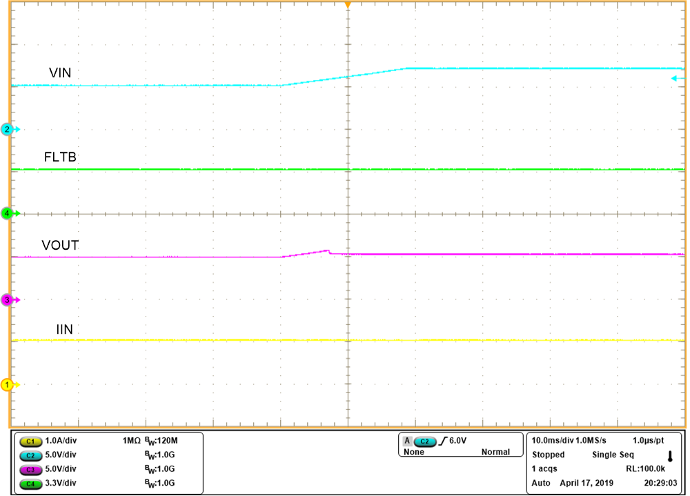
TPS2596 Waveform-OVC-5-7V.png
OVCSEL = 400 KΩ to GND, VIN increased from 5 V to 7 V
Figure 16. TPS25962x Overvoltage Clamp Response
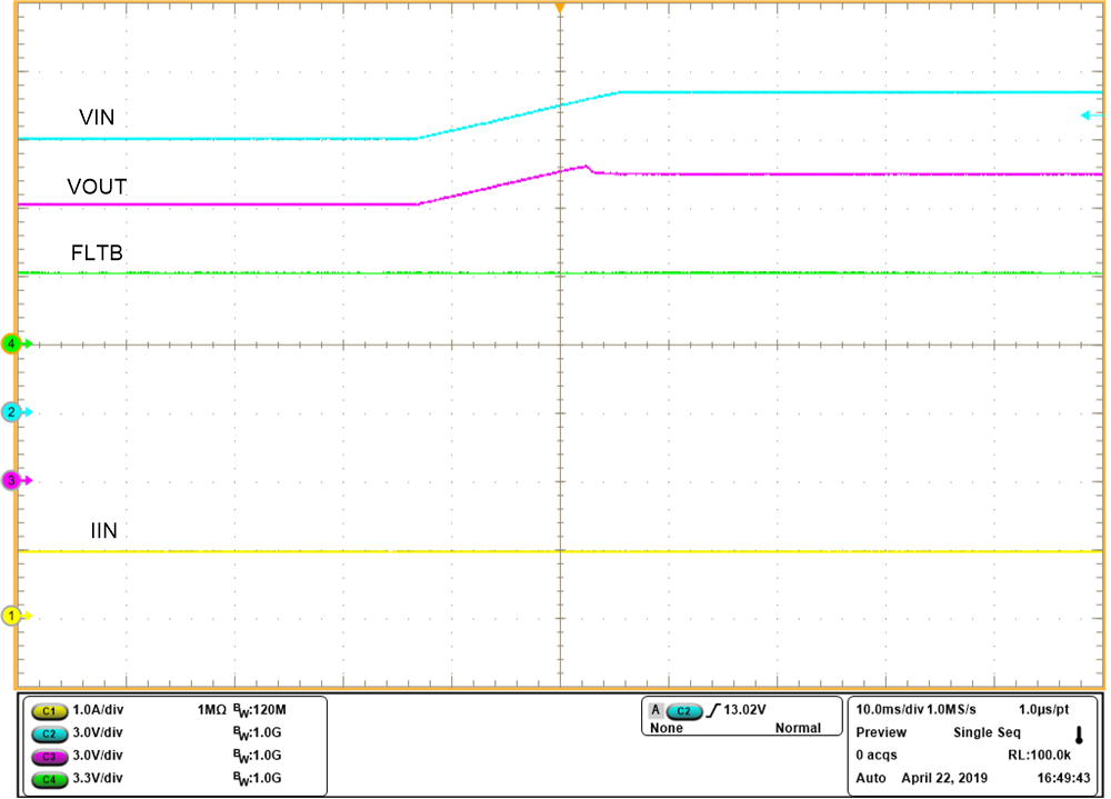
TPS2596 Waveform-OVC-13-8V.png
OVCSEL = OPEN, VIN increased from 12 V to 14 V
Figure 17. TPS25962x Overvoltage Clamp Response