JAJSHD7 May   2019 TPS2596

ADVANCE INFORMATION for pre-production products; subject to change without notice.  

  1. 特長
  2. アプリケーション
  3. 概要
    1.     Device Images
      1.      概略回路図
      2.      TPS25963x の 1kV EFT 応答
  4. 改訂履歴
  5. デバイス比較表
  6. Pin Configuration and Functions
    1. Table 1. Pin Functions
  7. Specifications
    1. 7.1 Absolute Maximum Ratings
    2. 7.2 ESD Ratings
    3. 7.3 Recommended Operating Conditions
    4. 7.4 Thermal Information
    5. 7.5 Electrical Characteristics
    6. 7.6 Timing Requirements
    7. 7.7 Switching Characteristics
    8. 7.8 Typical Characteristics
  8. Detailed Description
    1. 8.1 Overview
    2. 8.2 Feature Description
    3. 8.3 Functional Block Diagram
      1. 8.3.1 TPS25962x Block Diagram
      2. 8.3.2 TPS25963x Block Diagram
    4. 8.4 Feature Description
      1. 8.4.1 Undervoltage Protection (UVP) and Undervoltage Lockout (UVLO)
      2. 8.4.2 Overvoltage Protection
        1. 8.4.2.1 Overvoltage Lockout
        2. 8.4.2.2 Overvoltage Clamp
      3. 8.4.3 Inrush Current, Overcurrent and Short Circuit Protection
        1. 8.4.3.1 Slew Rate and Inrush Current Control (dVdt)
        2. 8.4.3.2 Active Current Limiting
        3. 8.4.3.3 Short Circuit Protection
      4. 8.4.4 Analog Load Current Monitor (IMON)
      5. 8.4.5 Overtemperature Protection (OTP)
      6. 8.4.6 Fault Indication
    5. 8.5 Device Functional Modes
      1. 8.5.1 Enable and Fault Pin Functional Mode 1: Single Device, Self-Controlled
      2. 8.5.2 Enable and Fault Pin Functional Mode 2: Single Device, Host-Controlled
      3. 8.5.3 Enable and Fault Pin Functional Mode 3: Multiple Devices, Self-Controlled
  9. Application and Implementation
    1. 9.1 Application Information
    2. 9.2 Typical Application
      1. 9.2.1 Precision Current Limiting and Protection for White Goods
      2. 9.2.2 Design Requirements
      3. 9.2.3 Detailed Design Procedure
        1. 9.2.3.1 Programming the Current-Limit Threshold: RILM Selection
        2. 9.2.3.2 Undervoltage and Overvoltage Lockout Set Point
        3. 9.2.3.3 Setting Output Voltage Ramp Time (TdVdT)
          1. 9.2.3.3.1 Case 1: Start-Up Without Load. Only Output Capacitance COUT Draws Current
          2. 9.2.3.3.2 Case 2: Start-Up With Load. Output Capacitance COUT and Load Draw Current
      4. 9.2.4 Support Component Selection: RFLT and CIN
      5. 9.2.5 Application Curves
    3. 9.3 System Examples
      1. 9.3.1 Current Limiting and Overvoltage Protection and for Energy Meter Power Rails
      2. 9.3.2 Precision Current Limiting and Protection in Appliances
  10. 10Power Supply Recommendations
    1. 10.1 Transient Protection
    2. 10.2 Output Short-Circuit Measurements
  11. 11Layout
    1. 11.1 Layout Guidelines
    2. 11.2 Layout Example
  12. 12デバイスおよびドキュメントのサポート
    1. 12.1 ドキュメントのサポート
      1. 12.1.1 関連資料
    2. 12.2 ドキュメントの更新通知を受け取る方法
    3. 12.3 コミュニティ・リソース
    4. 12.4 商標
    5. 12.5 静電気放電に関する注意事項
    6. 12.6 Glossary
  13. 13メカニカル、パッケージ、および注文情報

パッケージ・オプション

メカニカル・データ(パッケージ|ピン)
サーマルパッド・メカニカル・データ
発注情報

Overvoltage Lockout

The TPS25963x device provides an user programmable OVLO mechanism to ensure that the supply to the load is cut off if the input supply voltage exceeds a certain level. This can be achieved by dividing the input supply and feeding it to the OVLO pin. Whenever the voltage at the OVLO pin rises above a threshold VOVLO(R), the device turns OFF the FET. When the voltage at the OVLO pin falls below the threshold VOVLO(F), the FET is turned ON again. The rising and falling thresholds on this pin are slightly different, thereby providing some hysteresis and ensuring stable operation around the threshold voltage.
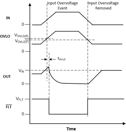
TPS2596 Timing-diagram-OVLO.gifFigure 19. TPS25963x Overvoltage Lockout Response

The user should choose the resistor divider values appropriately to map the desired input overvoltage level to the OVLO threshold of the part.
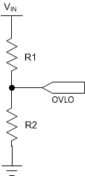
TPS2596 Circuit-OVLO-connection-TPS25963x.gifFigure 20. TPS25963x Programmable Overvoltage Lockout
Equation 2. TPS2596 Equation-OVLO.gif