JAJSHD7 May   2019 TPS2596

ADVANCE INFORMATION for pre-production products; subject to change without notice.  

  1. 特長
  2. アプリケーション
  3. 概要
    1.     Device Images
      1.      概略回路図
      2.      TPS25963x の 1kV EFT 応答
  4. 改訂履歴
  5. デバイス比較表
  6. Pin Configuration and Functions
    1. Table 1. Pin Functions
  7. Specifications
    1. 7.1 Absolute Maximum Ratings
    2. 7.2 ESD Ratings
    3. 7.3 Recommended Operating Conditions
    4. 7.4 Thermal Information
    5. 7.5 Electrical Characteristics
    6. 7.6 Timing Requirements
    7. 7.7 Switching Characteristics
    8. 7.8 Typical Characteristics
  8. Detailed Description
    1. 8.1 Overview
    2. 8.2 Feature Description
    3. 8.3 Functional Block Diagram
      1. 8.3.1 TPS25962x Block Diagram
      2. 8.3.2 TPS25963x Block Diagram
    4. 8.4 Feature Description
      1. 8.4.1 Undervoltage Protection (UVP) and Undervoltage Lockout (UVLO)
      2. 8.4.2 Overvoltage Protection
        1. 8.4.2.1 Overvoltage Lockout
        2. 8.4.2.2 Overvoltage Clamp
      3. 8.4.3 Inrush Current, Overcurrent and Short Circuit Protection
        1. 8.4.3.1 Slew Rate and Inrush Current Control (dVdt)
        2. 8.4.3.2 Active Current Limiting
        3. 8.4.3.3 Short Circuit Protection
      4. 8.4.4 Analog Load Current Monitor (IMON)
      5. 8.4.5 Overtemperature Protection (OTP)
      6. 8.4.6 Fault Indication
    5. 8.5 Device Functional Modes
      1. 8.5.1 Enable and Fault Pin Functional Mode 1: Single Device, Self-Controlled
      2. 8.5.2 Enable and Fault Pin Functional Mode 2: Single Device, Host-Controlled
      3. 8.5.3 Enable and Fault Pin Functional Mode 3: Multiple Devices, Self-Controlled
  9. Application and Implementation
    1. 9.1 Application Information
    2. 9.2 Typical Application
      1. 9.2.1 Precision Current Limiting and Protection for White Goods
      2. 9.2.2 Design Requirements
      3. 9.2.3 Detailed Design Procedure
        1. 9.2.3.1 Programming the Current-Limit Threshold: RILM Selection
        2. 9.2.3.2 Undervoltage and Overvoltage Lockout Set Point
        3. 9.2.3.3 Setting Output Voltage Ramp Time (TdVdT)
          1. 9.2.3.3.1 Case 1: Start-Up Without Load. Only Output Capacitance COUT Draws Current
          2. 9.2.3.3.2 Case 2: Start-Up With Load. Output Capacitance COUT and Load Draw Current
      4. 9.2.4 Support Component Selection: RFLT and CIN
      5. 9.2.5 Application Curves
    3. 9.3 System Examples
      1. 9.3.1 Current Limiting and Overvoltage Protection and for Energy Meter Power Rails
      2. 9.3.2 Precision Current Limiting and Protection in Appliances
  10. 10Power Supply Recommendations
    1. 10.1 Transient Protection
    2. 10.2 Output Short-Circuit Measurements
  11. 11Layout
    1. 11.1 Layout Guidelines
    2. 11.2 Layout Example
  12. 12デバイスおよびドキュメントのサポート
    1. 12.1 ドキュメントのサポート
      1. 12.1.1 関連資料
    2. 12.2 ドキュメントの更新通知を受け取る方法
    3. 12.3 コミュニティ・リソース
    4. 12.4 商標
    5. 12.5 静電気放電に関する注意事項
    6. 12.6 Glossary
  13. 13メカニカル、パッケージ、および注文情報

パッケージ・オプション

メカニカル・データ(パッケージ|ピン)
サーマルパッド・メカニカル・データ
発注情報

Active Current Limiting

The load current is monitored during start-up and normal operation. When the load current exceeds the current limit ILIM programmed by RILM resistor, the device regulates the current to the set limit ILIM within tLIM. The device exits current limiting when the load current falls below ILIM. Equation 5 can be used to find the RILM value for a desired current limit.

Equation 5. TPS2596 Equation-ILIM.gif

In the current limiting state, the output voltage drops resulting in increased power dissipation in the internal FET leading to a thermal shutdown if the condition persists for an extended period of time. In this case, the device either stays latched-off or starts an auto-retry cycle as explained in the Overtemperature Protection (OTP) section.
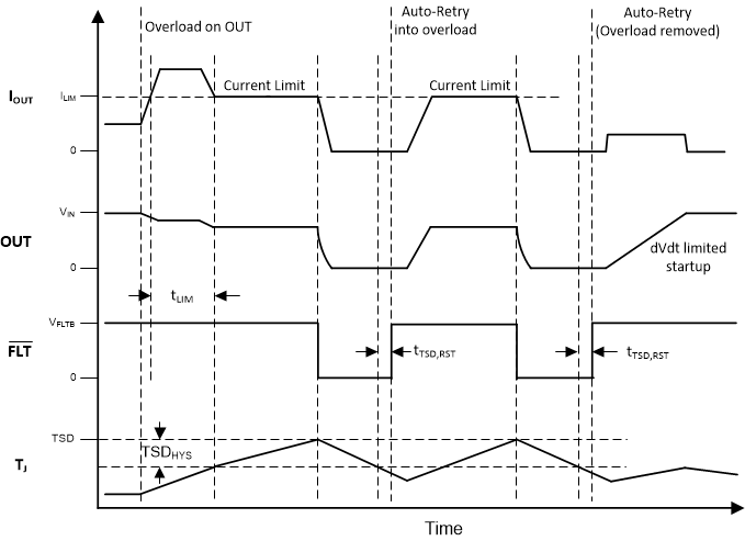
TPS2596 Timing-Diagram-CL-Retry.gifFigure 22. TPS2596x1 Overcurrent Response (Auto-retry)
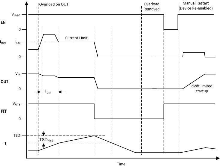
TPS2596 Timing-Diagram-CL-Latch-off.gifFigure 23. TPS2596x0 Overcurrent Response (Latch-off)