JAJSHD7 May 2019 TPS2596
ADVANCE INFORMATION for pre-production products; subject to change without notice.
- 1 特長
- 2 アプリケーション
- 3 概要
- 4 改訂履歴
- 5 デバイス比較表
- 6 Pin Configuration and Functions
- 7 Specifications
-
8 Detailed Description
- 8.1 Overview
- 8.2 Feature Description
- 8.3 Functional Block Diagram
- 8.4 Feature Description
- 8.5 Device Functional Modes
-
9 Application and Implementation
- 9.1 Application Information
- 9.2
Typical Application
- 9.2.1 Precision Current Limiting and Protection for White Goods
- 9.2.2 Design Requirements
- 9.2.3 Detailed Design Procedure
- 9.2.4 Support Component Selection: RFLT and CIN
- 9.2.5 Application Curves
- 9.3 System Examples
- 10Power Supply Recommendations
- 11Layout
- 12デバイスおよびドキュメントのサポート
- 13メカニカル、パッケージ、および注文情報
パッケージ・オプション
メカニカル・データ(パッケージ|ピン)
- DDA|8
サーマルパッド・メカニカル・データ
- DDA|8
発注情報
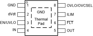
6 Pin Configuration and Functions
DDA Package
8-Pin SOIC
Top View

Table 1. Pin Functions
| PIN | I/O | DESCRIPTION | |
|---|---|---|---|
| NAME | NO. | ||
| GND | 1 | Ground | Ground |
| dVdt | 2 | Analog Output | A capacitor from this pin to GND sets the output turn on slew rate. Leave this pin floating for the fastest turn on slew rate. |
| EN/UVLO | 3 | Analog Input | Active High Enable for the Device. A resistor divider can be used to adjust the Undervoltage Lockout threshold. Do not leave floating. |
| IN | 4 | Power | Power Input |
| OUT | 5 | Power | Power Output |
| FLT | 6 | Digital Output | Active Low indicator which will be pulled low when a fault is detected. It is an open drain output that requires an external pull-up resistance. |
| ILM | 7 | Analog Output | This is a dual function pin used to limit and monitor the output current. An external resistor from this pin to GND sets the output current limit. The pin voltage can also be used to monitor the output load current. |
| OVLO (TPS25963x) | 8 | Analog Input | A resistor divider can be used to adjust the Overvoltage Lockout threshold. Do not leave floating. |
| OVCSEL (TPS25962x) | Overvoltage Clamp voltage select pin. Refer to Overvoltage Clamp for more details. | ||
| Thermal pad | Ground | The Exposed Pad is used primarily for heat dissipation and must be connected to system ground plane. | |