JAJSMF6C november 2021 – april 2023 TPS2597
PRODUCTION DATA
- 1 特長
- 2 アプリケーション
- 3 概要
- 4 Revision History
- 5 Device Comparison Table
- 6 Pin Configuration and Functions
- 7 Specifications
-
8 Detailed Description
- 8.1 Overview
- 8.2 Functional Block Diagram
- 8.3
Feature Description
- 8.3.1 Undervoltage Lockout (UVLO and UVP)
- 8.3.2 Overvoltage Lockout (OVLO)
- 8.3.3 Overvoltage Clamp (OVC)
- 8.3.4 Inrush Current, Overcurrent, and Short Circuit Protection
- 8.3.5 Analog Load Current Monitor
- 8.3.6 Overtemperature Protection (OTP)
- 8.3.7 Fault Response and Indication (FLT)
- 8.3.8 Power-Good Indication (PG)
- 8.4 Device Functional Modes
- 9 Application and Implementation
- 10Device and Documentation Support
- 11Mechanical, Packaging, and Orderable Information
8.3.8 Power-Good Indication (PG)
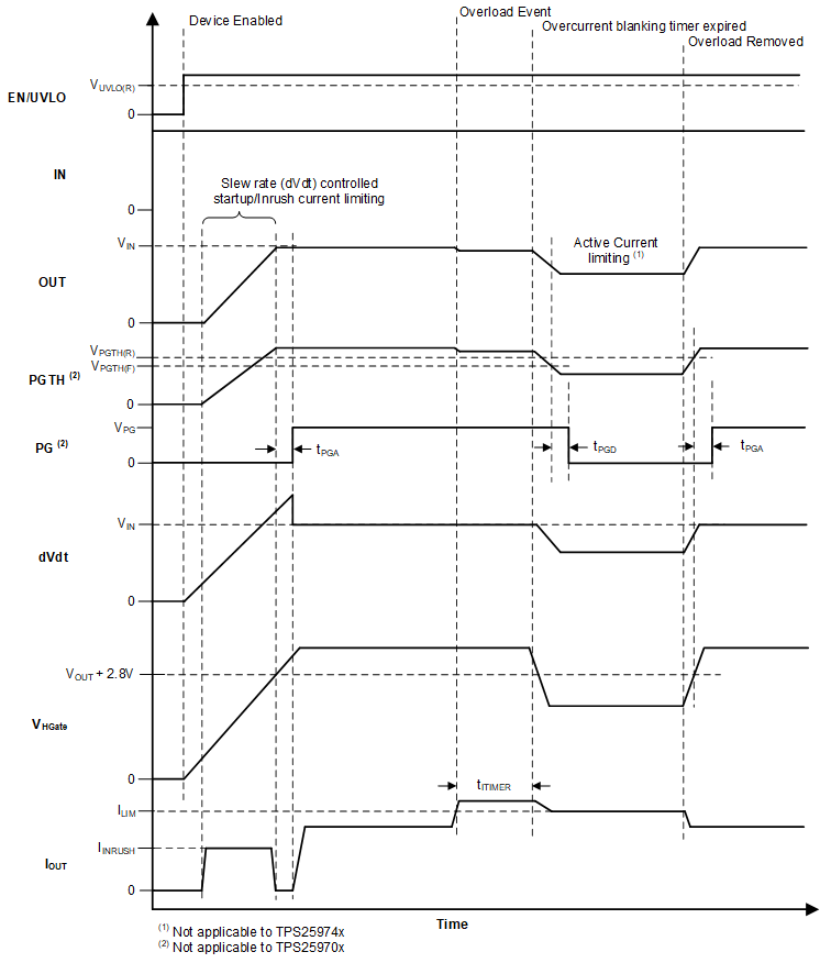
The TPS25972x and TPS25974x variants provide an active high digital output (PG) which serves as a power-good indication signal and is asserted high depending on the voltage at the PGTH pin along with the device state information. The PG is an open-drain pin and must be pulled up to an external supply.
After power up, PG is pulled low initially. The device initiates a inrush sequence in which the HFET is turned on in a controlled manner. When the HFET gate voltage reaches the full overdrive indicating that the inrush sequence is complete and the voltage at PGTH is above VPGTH(R), the PG is asserted after a de-glitch time (tPGA).
PG is de-asserted if at any time during normal operation, the voltage at PGTH falls below VPGTH(F), or the device detects a fault (except overcurrent). The PG de-assertion de-glitch time is tPGD.
 Figure 8-13 TPS25972x, TPS25974x PG Timing
Diagram
Figure 8-13 TPS25972x, TPS25974x PG Timing
Diagram|
EVENT |
DEVICE STATUS |
PG PIN STATUS |
PG PIN TOGGLE DELAY |
|---|---|---|---|
|
Undervoltage (UVP or UVLO) |
OFF |
L |
|
|
Overvoltage (TPS25972x only) |
ON (Clamping) |
H (If PGTH pin voltage > VPGTH(R)) L (If PGTH pin voltage < VPGTH(F)) |
tPGA tPGD |
|
Overvoltage (TPS25974x only) |
OFF |
L |
tPGD |
|
Steady state |
ON |
H (If PGTH pin voltage > VPGTH(R)) L (If PGTH pin voltage < VPGTH(F)) |
tPGA tPGD |
|
Transient overcurrent |
ON |
H (If PGTH pin voltage > VPGTH(R)) L (If PGTH pin voltage < VPGTH(F)) |
tPGA tPGD |
|
Persistent overload (TPS25972x only) |
ON (Current Limiting) |
H (If PGTH pin voltage > VPGTH(R)) L (If PGTH pin voltage < VPGTH(F)) |
tPGA tPGD |
|
Persistent overload (TPS25974x only) |
OFF (Circuit-Breaker) |
L |
tPGD |
|
Output short-circuit to GND |
Fast-trip followed by Current Limit |
H (If PGTH pin voltage > VPGTH(R)) L (If PGTH pin voltage < VPGTH(F)) |
tPGA tPGD |
|
ILM pin open |
OFF |
L (If PGTH < 1.1 V) |
tPGD + tITIMER |
|
ILM pin shorted to GND |
OFF |
L |
tPGD |
|
Overtemperature |
OFF |
L |
tPGD |
When there is no supply to the device, the PG pin is expected to stay low. However, there is no active pulldown in this condition to drive this pin all the way down to 0 V. If the PG pin is pulled up to an independent supply which is present even if the device is unpowered, there can be a small voltage seen on this pin depending on the pin sink current, which is a function of the pullup supply voltage and resistor. Minimize the sink current to keep this pin voltage low enough not to be detected as a logic HIGH by associated external circuits in this condition.