JAJSMF6C november 2021 – april 2023 TPS2597
PRODUCTION DATA
- 1 特長
- 2 アプリケーション
- 3 概要
- 4 Revision History
- 5 Device Comparison Table
- 6 Pin Configuration and Functions
- 7 Specifications
-
8 Detailed Description
- 8.1 Overview
- 8.2 Functional Block Diagram
- 8.3
Feature Description
- 8.3.1 Undervoltage Lockout (UVLO and UVP)
- 8.3.2 Overvoltage Lockout (OVLO)
- 8.3.3 Overvoltage Clamp (OVC)
- 8.3.4 Inrush Current, Overcurrent, and Short Circuit Protection
- 8.3.5 Analog Load Current Monitor
- 8.3.6 Overtemperature Protection (OTP)
- 8.3.7 Fault Response and Indication (FLT)
- 8.3.8 Power-Good Indication (PG)
- 8.4 Device Functional Modes
- 9 Application and Implementation
- 10Device and Documentation Support
- 11Mechanical, Packaging, and Orderable Information
9.3 Parallel Operation
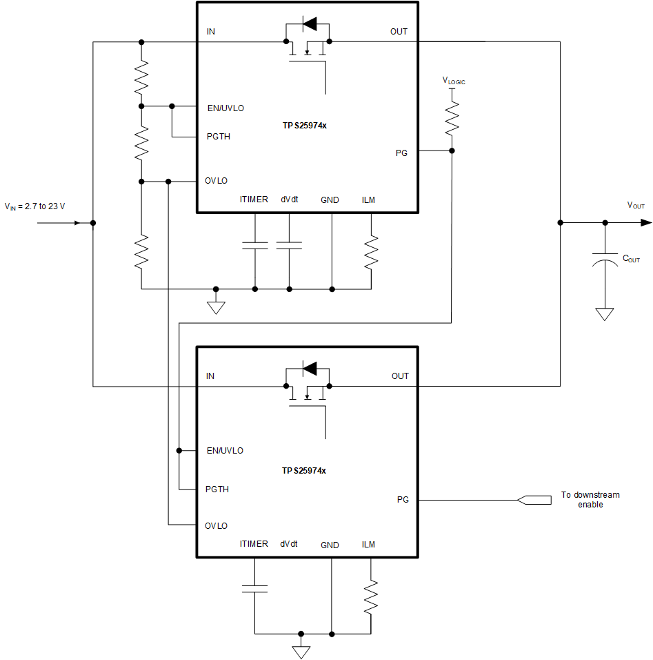
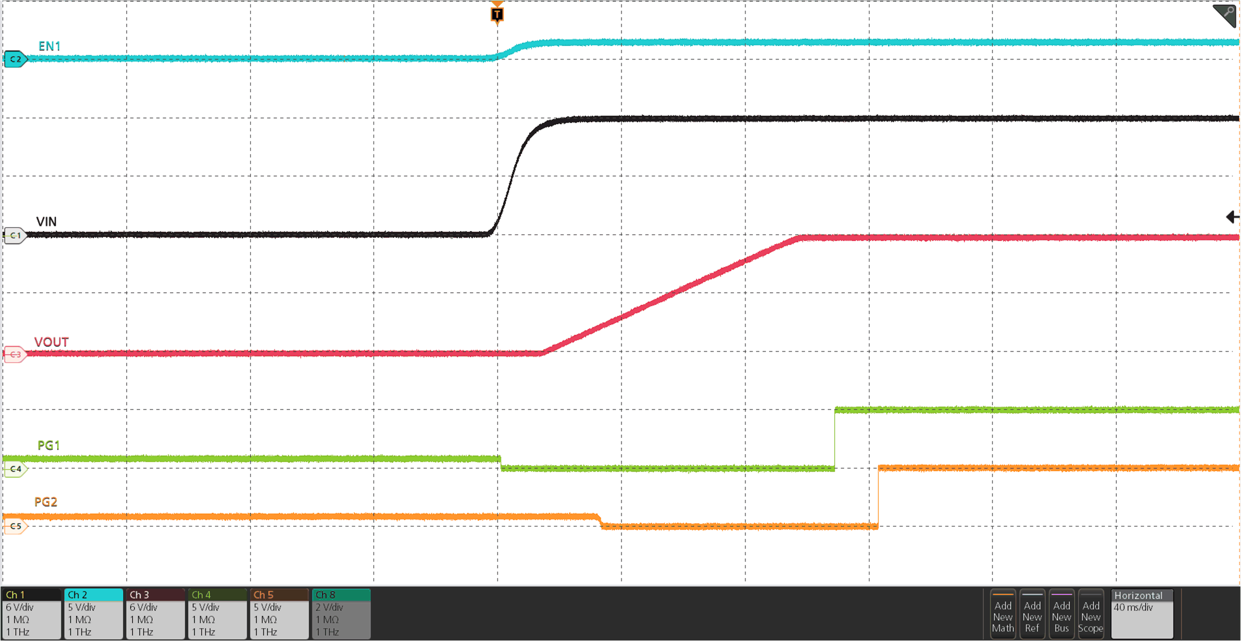
Applications that need higher steady current can use two TPS25974x devices connected in parallel as shown in Figure 9-20. In this configuration, the first device turns on initially to provide the inrush current control. The second device is held in an OFF state by driving its EN/UVLO pin low using the PG signal of the first device. After the inrush sequence is complete, the first device asserts its PG pin high and turns on the second device. The second device asserts its PG signal to indicate when it has turned on fully, thereby indicating to the system that the parallel combination is ready to deliver the full steady state current.
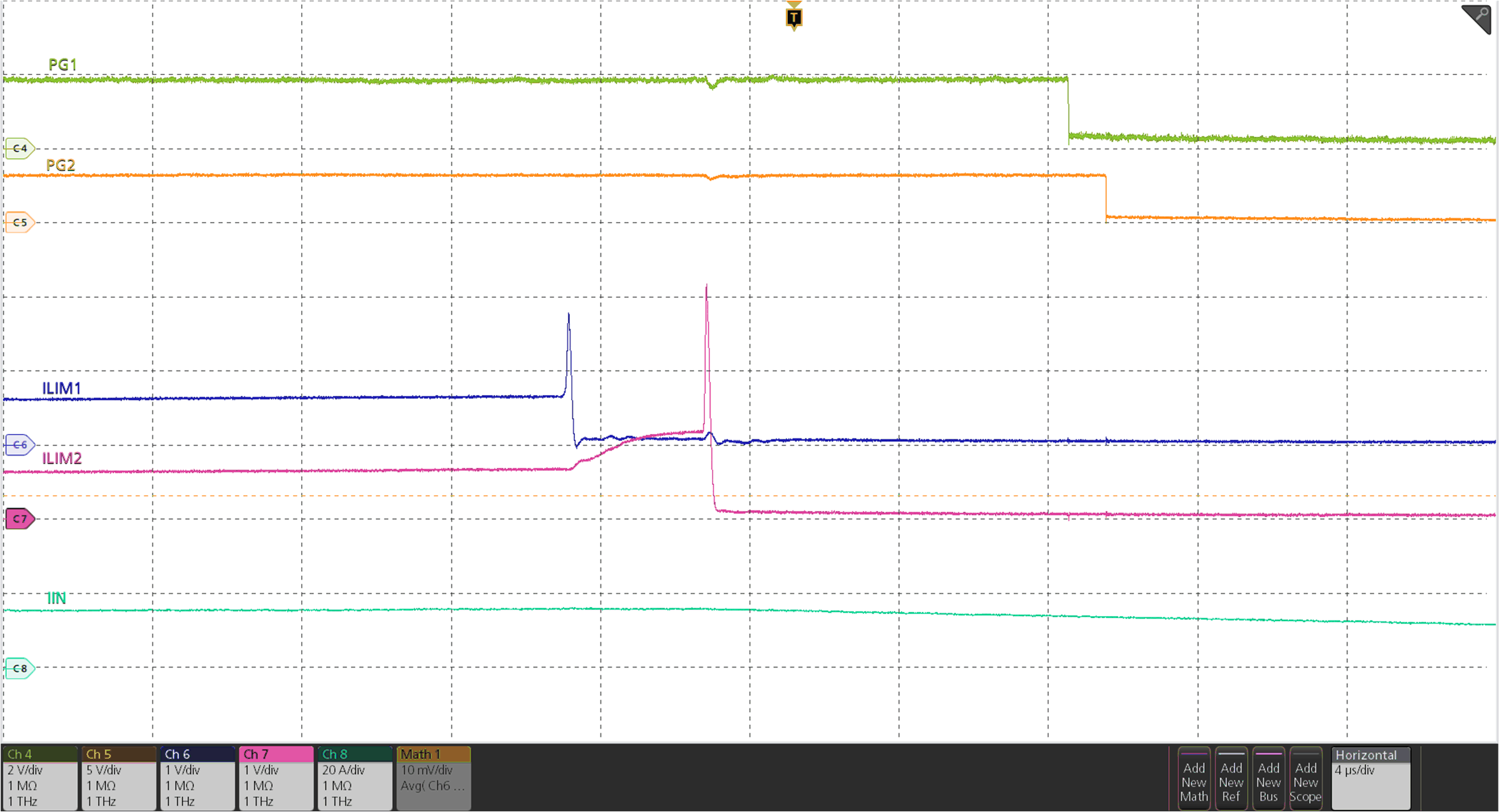
After in steady state, both devices share current nearly equally. There can be a slight skew in the currents depending on the part-to-part variation in the RON as well as the PCB trace resistance mismatch.
 Figure 9-7 Two Devices Connected in
Parallel for Higher Steady State Current Capability
Figure 9-7 Two Devices Connected in
Parallel for Higher Steady State Current CapabilityThe waveforms below illustrate the behavior of the parallel configuration during start-up as well as during steady state.
 Figure 9-8 Parallel Devices Sequencing
During Start-Up
 Figure 9-9 Parallel Devices Load Current
During Steady State and Overload