JAJSJ14 August   2020 TPS25980

PRODUCTION DATA  

  1. 特長
  2. アプリケーション
  3. 概要
  4. Revision History
  5. Device Comparison Table
  6. Pin Configuration and Functions
    1.     7
  7. Specifications
    1. 7.1 Absolute Maximum Ratings
    2. 7.2 ESD Ratings
    3. 7.3 Recommended Operating Conditions
    4. 7.4 Thermal Information
    5. 7.5 Electrical Characteristics
    6. 7.6 Timing Requirements
    7. 7.7 Switching Characteristics
    8. 7.8 Typical Characteristics
  8. Detailed Description
    1. 8.1 Overview
    2. 8.2 Functional Block Diagram
    3. 8.3 Feature Description
      1. 8.3.1 Undervoltage Protection (UVLO and UVP)
      2. 8.3.2 Overvoltage Protection (OVP)
      3. 8.3.3 Inrush Current, Overcurrent, and Short-Circuit Protection
        1. 8.3.3.1 Slew Rate and Inrush Current Control (dVdt)
        2. 8.3.3.2 Circuit Breaker
        3. 8.3.3.3 Short-Circuit Protection
      4. 8.3.4 Overtemperature Protection (OTP)
      5. 8.3.5 Analog Load Current Monitor (IMON)
      6. 8.3.6 Power Good (PG)
      7. 8.3.7 Load Detect/Handshake (LDSTRT)
    4. 8.4 Fault Response
    5. 8.5 Device Functional Modes
  9. Application and Implementation
    1. 9.1 Application Information
    2. 9.2 Typical Application: Patient Monitoring System in Medical Applications
      1. 9.2.1 Design Requirements
      2. 9.2.2 Detailed Design Procedure
        1. 9.2.2.1 Device Selection
        2. 9.2.2.2 Setting the Current Limit Threshold: RILIM Selection
        3. 9.2.2.3 Setting the Undervoltage Lockout Set Point
        4. 9.2.2.4 Choosing the Current Monitoring Resistor: RIMON
        5. 9.2.2.5 Setting the Output Voltage Ramp Time (TdVdt)
          1. 9.2.2.5.1 Case 1: Start-Up Without Load: Only Output Capacitance COUT Draws Current
          2. 9.2.2.5.2 Case 2: Start-Up With Load: Output Capacitance COUT and Load Draw Current
        6. 9.2.2.6 Setting the Load Handshake (LDSTRT) Delay
        7. 9.2.2.7 Setting the Transient Overcurrent Blanking Interval (tITIMER)
        8. 9.2.2.8 Setting the Auto-Retry Delay and Number of Retries
      3. 9.2.3 Application Curves
    3. 9.3 System Examples
      1. 9.3.1 Optical Module Power Rail Path Protection
        1. 9.3.1.1 Design Requirements
        2. 9.3.1.2 Device Selection
        3. 9.3.1.3 External Component Settings
        4. 9.3.1.4 Voltage Drop
        5. 9.3.1.5 Application Curves
      2. 9.3.2 Input Protection for 12-V Rail Applications: PCIe Cards, Storage Interfaces and DC Fans
  10. 10Power Supply Recommendations
    1. 10.1 Transient Protection
    2. 10.2 Output Short-Circuit Measurements
  11. 11Layout
    1. 11.1 Layout Guidelines
    2. 11.2 Layout Example
  12. 12Device and Documentation Support
    1. 12.1 Documentation Support
      1. 12.1.1 Related Documentation
        1. 12.1.1.1 Related Links
    2. 12.2 Receiving Notification of Documentation Updates
    3. 12.3 Support Resources
    4. 12.4 Trademarks
    5. 12.5 静電気放電に関する注意事項
    6. 12.6 Glossary
  13. 13Mechanical, Packaging, and Orderable Information

パッケージ・オプション

メカニカル・データ(パッケージ|ピン)
サーマルパッド・メカニカル・データ
発注情報

Overvoltage Protection (OVP)

The TPS25980x implements Overvoltage Lock-Out (OVLO) on IN to protect the output load in the event of input overvoltage. When the input exceeds the Overvoltage Protection threshold (VOVP(R)) the device turns off the output within tOVP. As long as an overvoltage condition is present on the input, the device stays disabled and the output will be turned off. Once the input voltage returns to the normal operating range, the device attempts to start up normally.
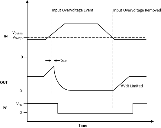
GUID-15419069-F137-4332-9998-486F89B84F07-low.gifFigure 8-2 Overvoltage Response

There are multiple device options with different fixed overvoltage thresholds to choose from, including one without internal overvoltage protection. See the Device Comparison Table for a list of available options.