JAJSMF7B april 2022 – june 2023 TPS25981
PRODUCTION DATA
- 1
- 1 特長
- 2 アプリケーション
- 3 概要
- 4 Revision History
- 5 Device Comparison Table
- 6 Pin Configuration and Functions
- 7 Specifications
-
8 Detailed Description
- 8.1 Overview
- 8.2 Functional Block Diagram
- 8.3
Feature Description
- 8.3.1 Undervoltage Lockout (UVLO and UVP)
- 8.3.2 Overvoltage Lockout (OVLO)
- 8.3.3 Inrush Current, Overcurrent, and Short-Circuit Protection
- 8.3.4 Analog Load Current Monitor
- 8.3.5 Overtemperature Protection (OTP)
- 8.3.6 Fault Response and Indication (FLT)
- 8.3.7 Power Good Indication (PG)
- 8.3.8 Quick Output Discharge (QOD)
- 8.3.9 Reverse Current Blocking FET Driver
- 8.4 Device Functional Modes
- 9 Application and Implementation
- 10Power Supply Recommendations
- 11Layout
- 12Device and Documentation Support
- 13Mechanical, Packaging, and Orderable Information
8.3.3.2 Circuit-Breaker During Steady-State
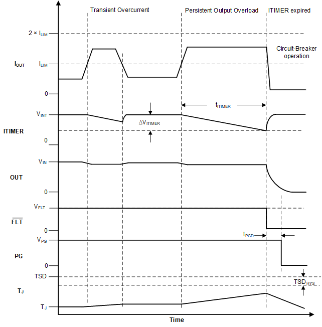
The TPS259814x (circuit-breaker) variants respond to output overcurrent conditions by turning off the output after a user adjustable transient fault blanking interval. When the load current exceeds the set overcurrent threshold (ILIM) set by the ILM pin resistor (RILM), but stays lower than the fast-trip threshold (2 × ILIM), the device starts discharging the ITIMER pin capacitor using an internal 2-μA pulldown current. If the load current drops below ILIM before the ITIMER pin capacitor (CITIMER) discharges by ΔVITIMER, the ITIMER is reset by pulling it up to VINT internally and the circuit-breaker action is not engaged. This action allows short load transient pulses to pass through the device without tripping the circuit. If the overcurrent condition persists, the CITIMER continues to discharge and after it discharges by ΔVITIMER, the circuit-breaker action turns off the FET immediately. At the same time, the CITIMER is charged up to VINT again so that it is at its default state before the next overcurrent event. This action ensures the full blanking timer interval is provided for every overcurrent event. Equation 5 can be used to calculate the RILM value for a overcurrent threshold.
Leaving the ILM pin open sets the current limit to nearly zero and results in the part breaking the circuit with the slightest amount of loading at the output.
Shorting the ILM pin to ground at any point during normal operation is detected as a fault and the part shuts down. There is a minimum current (IFLT) which the part allows in this condition before the pin short condition is detected.
The duration for which transients are allowed can be adjusted using an appropriate capacitor value from ITIMER pin to ground. Use Equation 6 to calculate the CITIMER value needed to set the desired transient overcurrent blanking interval.
 Figure 8-4 TPS259814x Overcurrent Response
 - Leave the ITIMER pin open to allow the part to break the circuit with the minimum possible delay.
- Shorting the ITIMER pin to ground results in minimum overcurrent response delay (similar to ITIMER pin open condition), but increases the device current consumption. This action is not a recommended mode of operation.
- Increasing the ITIMER cap value extends the overcurrent blanking interval, but it also extends the time needed for the CITIMER to recharge up to VINT. If the next overcurrent event occurs before the CITIMER is recharged fully, it takes lesser time to discharge to the ITIMER expiry threshold, thereby providing a shorter blanking interval than intended.
In low voltage applications, TI recommends adding a 30 kΩ resistor between the ITIMER pin and CITIMER for improved immunity to supply noise or fluctuations.
After the part shuts down due to a circuit-breaker fault, it either stays latched off (TPS259814L variant) or restarts automatically after a fixed delay (TPS259814A variant).