JAJSKF6C November 2020 – December 2021 TPS2661
PRODUCTION DATA
- 1 特長
- 2 アプリケーション
- 3 概要
- 4 Revision History
- 5 Device Comparison Table
- 6 Pin Configuration and Functions
- 7 Specifications
-
8 Detailed Description
- 8.1 Overview
- 8.2 Functional Block Diagram
- 8.3
Feature Description
- 8.3.1 Overload Protection and Fast-Trip
- 8.3.2 Reverse Current Blocking for Unipolar Current Inputs TPS26610, TPS26611 and TPS26612 (4–20 mA, 0–20 mA)
- 8.3.3 OUTPUT and INPUT Cutoff During Overvoltage, Undervoltage Due to Miswiring
- 8.3.4 External Power Supply (±Vs)
- 8.3.5 Loop Testing Without ±Vs Supply (Loop Power Mode in TPS26610, TPS26613 Only)
- 8.3.6 Enable Control With TPS26611, TPS26612, and TPS26614
- 8.3.7 Signal Good Indicator (SGOOD)
- 8.4 Device Functional Modes
-
9 Application and Implementation
- 9.1 Application Information
- 9.2 Typical Application: Analog Input Protection for Current Inputs with TPS26610
- 9.3 Typical Application: Analog Input Protection for Multiplexed Current and Voltage Inputs with TPS26611
- 9.4 System Examples
- 10Power Supply Recommendations
- 11Layout
- 12Device and Documentation Support
- 13Mechanical, Packaging, and Orderable Information
9.4.1 Power Supply Protection of 2-Wire Transmitter with TPS26612
 Figure 9-11 Power Supply Protection for
2-Wire Transmitter with TPS26612
Figure 9-11 Power Supply Protection for
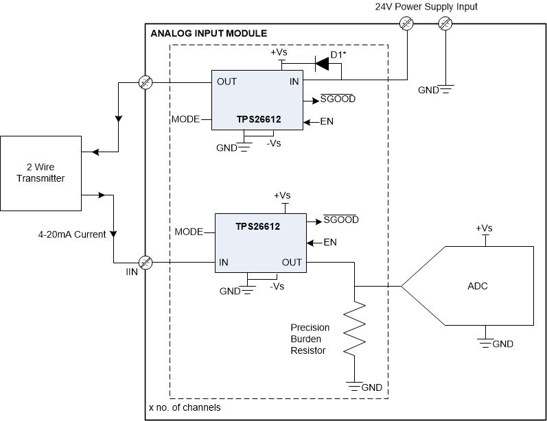
2-Wire Transmitter with TPS26612TPS26612 can be used for protection of power supply powering a two wire field transmitter as shown in Figure 9-11. Connect an external signal diode (D1) from IN to +Vs pin of TPS26612 in case of external field supply to protect the system from miswiring. In case the supply is internal to the module and miswiring is not a possibility, the signal diode (D1) is not needed. TPS26612 device includes higher threshold for overvoltage protection on OUT to accommodate the voltage drop of diode (D1) between IN and +Vs.
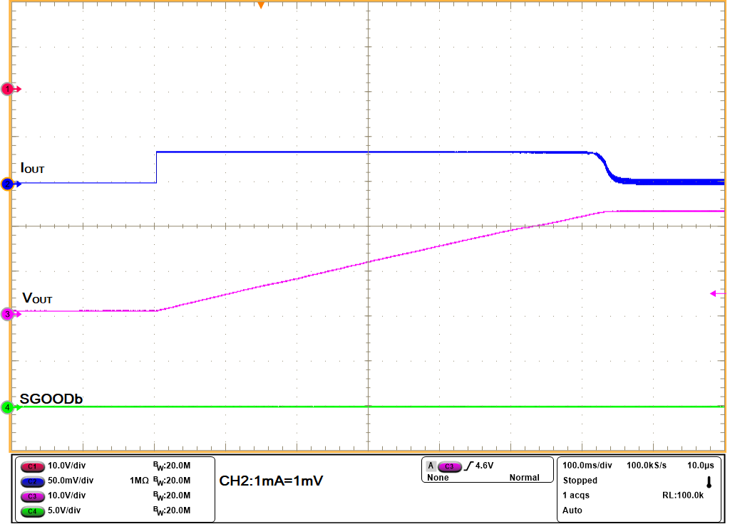
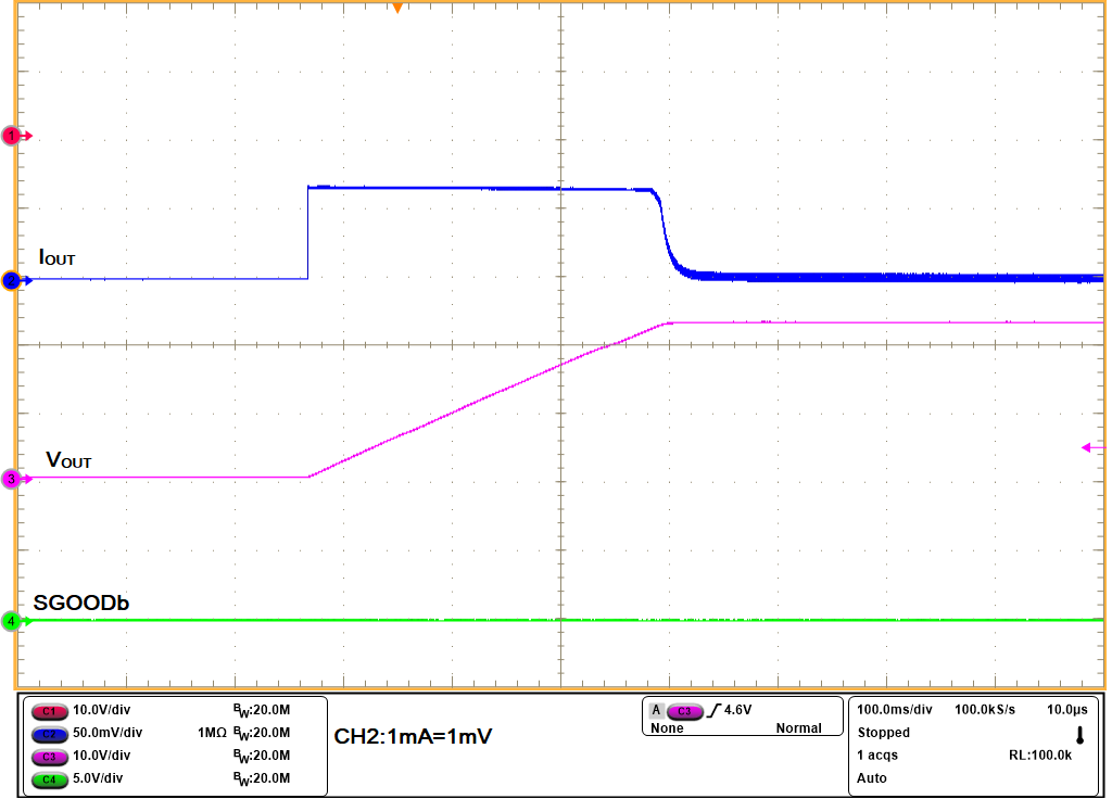
TPS26612 has over-load expiry time (tOL_expiry) disabled for the first overload fault after power-up up to a duration of tAR_dis (5 sec). With overload expiry time disabled, TPS26612 is able to power up 2-wire transmitters requiring higher start-up for longer durations (up to 5 sec.). The current limit threshold (IOL or 2 x IOL) for startup can be selected by MODE pin.

| VIN = 24 V, COUT = 1 mF |

| VIN = 24 V, COUT = 1 mF |
During the first overload fault, if the junction temperature reaches TSD, the device turns off the internal FETs and turns on as the junction temperature goes below [TTSD – TTSDHyst].