JAJSKF6C November 2020 – December 2021 TPS2661
PRODUCTION DATA
- 1 特長
- 2 アプリケーション
- 3 概要
- 4 Revision History
- 5 Device Comparison Table
- 6 Pin Configuration and Functions
- 7 Specifications
-
8 Detailed Description
- 8.1 Overview
- 8.2 Functional Block Diagram
- 8.3
Feature Description
- 8.3.1 Overload Protection and Fast-Trip
- 8.3.2 Reverse Current Blocking for Unipolar Current Inputs TPS26610, TPS26611 and TPS26612 (4–20 mA, 0–20 mA)
- 8.3.3 OUTPUT and INPUT Cutoff During Overvoltage, Undervoltage Due to Miswiring
- 8.3.4 External Power Supply (±Vs)
- 8.3.5 Loop Testing Without ±Vs Supply (Loop Power Mode in TPS26610, TPS26613 Only)
- 8.3.6 Enable Control With TPS26611, TPS26612, and TPS26614
- 8.3.7 Signal Good Indicator (SGOOD)
- 8.4 Device Functional Modes
-
9 Application and Implementation
- 9.1 Application Information
- 9.2 Typical Application: Analog Input Protection for Current Inputs with TPS26610
- 9.3 Typical Application: Analog Input Protection for Multiplexed Current and Voltage Inputs with TPS26611
- 9.4 System Examples
- 10Power Supply Recommendations
- 11Layout
- 12Device and Documentation Support
- 13Mechanical, Packaging, and Orderable Information
8.4 Device Functional Modes
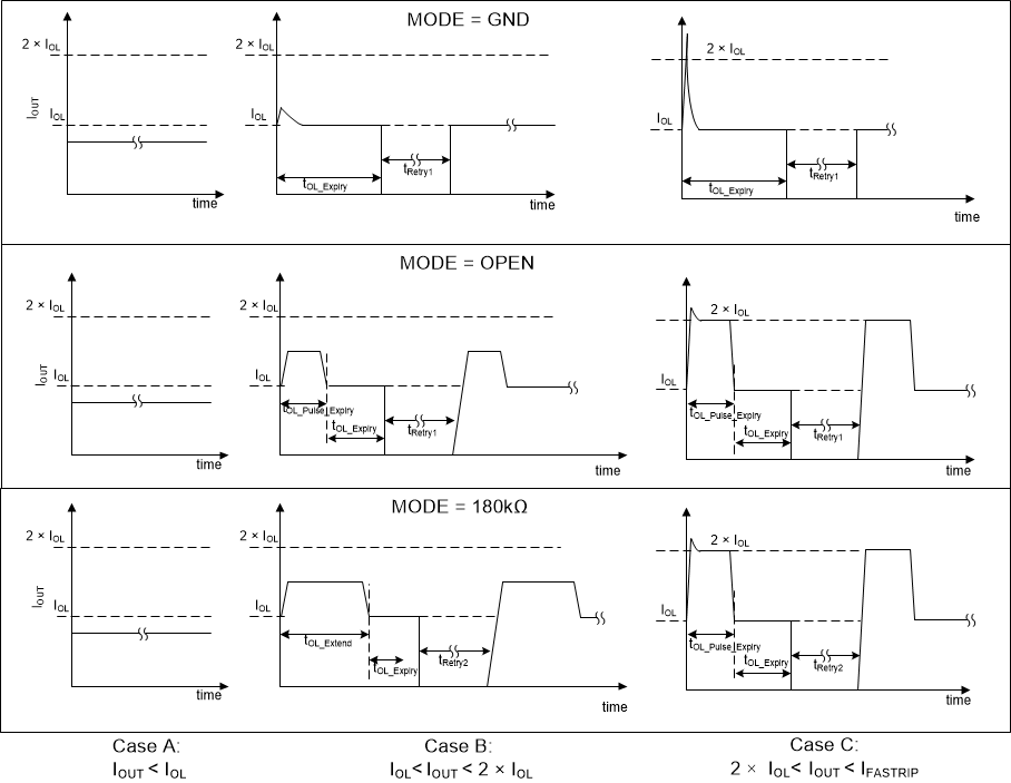
The device can provide higher current up to 2 × IOL for short durations. MODE pin of the device configures the behavior of the device for higher current. Table 8-3 and Figure 8-24 describe the device behavior in different modes for IOL > 0.
With MODE = GND, the device limits the current to IOL value for IOUT > IOL.
With MODE = OPEN, the device limits the output current as:
- For IOL < IOUT < 2 × IOL, the device allows current up to 2 × IOL for a duration of tOL_Pulse_Expiry and then limits the current to IOL value for a duration tOL_Expiry.
- For 2 × IOL < IOUT < I(FASTRIP), the device limits the current 2 × IOL value and for a duration of tOL_Pulse_Expiry and then limits the current to IOL value for a duration tOL_Expiry.
With MODE = 180 kΩ, the device limits the output current as:
- For IOL< IOUT < 2 × IOL, the device allows current up to 2 × IOL for a duration of tOL_Extend and then limits the current to IOL value for a duration tOL_Expiry.
- For 2 × IOL < IOUT < I(FASTRIP), the device limits the current 2 × IOL value and for a duration of tOL_Pulse_Expiry and then limits the current to IOL value for a duration tOL_Expiry.
Table 8-3 Device Operation Under Different MODE
Configurations for IOL > 0
| MODE Pin Configuration | IOUT < IOL (32 mA) | IOL (32 mA) < IOUT < 2 × IOL (60 mA) | 2 × IOL (60 mA) < IOUT < I(FASTRIP) | Auto-Retry Time |
|---|---|---|---|---|
| Shorted to GND | Current flows normally | Current limited to IOL for a duration of tOL_Expiry (100 ms). tOL_Expiry (100 ms) timer starts when IOUT exceeds IOL. | Current limited to IOL for a duration of tOL_Expiry (100
ms). tOL_Expiry (100 ms) timer starts when IOUT exceed IOL. | tRETRY1 (800 ms) |
| Open | Current flows normally | Device allows current for tOL_Pulse_Expiry (50 ms) time after which it
is limited to IOL for tOL_Expiry (100 ms) time
and then auto retry. tOL_Pulse_Expiry (50 ms) timer starts when IOUT exceeds IOL. | Current limited to 2 × IOL for tOL_Pulse_Expiry (50 ms)
time after which it is limited to IOL for
tOL_Expiry (100 ms) time and then auto retry. tOL_Pulse_Expiry (50 ms) timer starts when IOUT exceeds IOL. | tRETRY1 (800 ms) |
| 180 kΩ from MODE to GND | Current flows normally | Device allows current for tOL_Extend (5 s) time after which it is limited to
IOL for tOL_Expiry (100 ms) time and then
auto retry. tOL_Extend (5 s) timer starts when IOUT exceeds IOL. | Current limited to 2 × IOL for tOL_Pulse_Expiry (50 ms)
time after which it is limited to IOL for
tOL_Expiry (100 ms) time and then auto retry. tOL_Pulse_Expiry (50ms) timer starts when IOUT exceeds IOL. | tRETRY2 (1.6 s) |
 Figure 8-24 Device Operation Under Different MODE
Configurations for IOL > 0
Figure 8-24 Device Operation Under Different MODE
Configurations for IOL > 0Table 8-4 and Figure 8-25 describe the device behavior in different modes for IOL < 0.
Table 8-4 Device Operation Under Different MODE Configurations for IOL <
0
| MODE Pin Configuration | IOUT > –IOL (–32 mA) | –2 × IOL(–60 mA) < IOUT < –IOL (–32 mA) | –I(FASTRIP) < IOUT < –2 × IOL (–60 mA) | Auto-Retry Time |
|---|---|---|---|---|
| Shorted to GND or Open or 180 kΩ from MODE to GND | Current flows normally | Current limited to IOL for a duration
of tOL_Expiry (100 ms). tOL_Expiry (100 ms) timer starts when IOUT exceeds IOL. |
Current limited to IOL for a duration of tOL_Expiry (100ms). tOL_Expiry (100ms) timer starts when IOUT exceed IOL. | tRETRY1 (800 ms) |
 Figure 8-25 Device Operation Under
Different MODE Configurations for IOL < 0