JAJSGA2F September   2018  – June 2021 TPS2663

PRODUCTION DATA  

  1. 特長
  2. アプリケーション
  3. 概要
  4. Revision History
  5. Device Comparison Table
  6. Pin Configuration and Functions
  7. Specifications
    1. 7.1 Absolute Maximum Ratings
    2. 7.2 ESD Ratings
    3. 7.3 Recommended Operating Conditions
    4. 7.4 Thermal Information
    5. 7.5 Electrical Characteristics
    6. 7.6 Timing Requirements
    7. 7.7 Typical Characteristics
  8. Parameter Measurement Information
  9. Detailed Description
    1. 9.1 Overview
    2. 9.2 Functional Block Diagram
    3. 9.3 Feature Description
      1. 9.3.1  Hot Plug-In and In-Rush Current Control
        1. 9.3.1.1 Thermal Regulation Loop
      2. 9.3.2  PGOOD and PGTH
        1. 9.3.2.1 PGTH as VOUT Sensing Input
      3. 9.3.3  Undervoltage Lockout (UVLO)
      4. 9.3.4  Overvoltage Protection (OVP)
      5. 9.3.5  Input Reverse Polarity Protection (B_GATE, DRV)
      6. 9.3.6  Reverse Current Protection
      7. 9.3.7  Overload and Short Circuit Protection
        1. 9.3.7.1 Overload Protection
          1. 9.3.7.1.1 Active Current Limiting at 1x IOL, (TPS26630 and TPS26632 Only)
          2. 9.3.7.1.2 Active Current Limiting with 2x IOL Pulse Current Support, (TPS26631, TPS26633, TPS26635 and TPS26636 Only)
        2. 9.3.7.2 Short Circuit Protection
          1. 9.3.7.2.1 Start-Up With Short-Circuit On Output
      8. 9.3.8  Output Power Limiting, PLIM (TPS26632, TPS26633, TPS26635 and TPS26636 Only)
      9. 9.3.9  Current Monitoring Output (IMON)
      10. 9.3.10 FAULT Response ( FLT)
      11. 9.3.11 IN_SYS, IN, OUT and GND Pins
      12. 9.3.12 Thermal Shutdown
      13. 9.3.13 Low Current Shutdown Control (SHDN)
    4. 9.4 Device Functional Modes
  10. 10Application and Implementation
    1. 10.1 Application Information
    2. 10.2 Typical Application: Power Path Protection in a PLC System
      1. 10.2.1 Design Requirements
      2. 10.2.2 Detailed Design Procedure
        1. 10.2.2.1 Programming the Current-Limit Threshold—R(ILIM) Selection
        2. 10.2.2.2 Undervoltage Lockout and Overvoltage Set Point
        3. 10.2.2.3 Output Buffer Capacitor – COUT
        4. 10.2.2.4 PGTH Set Point
        5. 10.2.2.5 Setting Output Voltage Ramp Time—(tdVdT)
          1. 10.2.2.5.1 Support Component Selections— RPGOOD and C(IN)
        6. 10.2.2.6 Selecting Q1, Q2 and TVS Clamp for Surge Protection
      3. 10.2.3 Application Curves
    3. 10.3 System Examples
      1. 10.3.1 Simple 24-V Power Supply Path Protection
      2. 10.3.2 Priority Power MUX Operation
      3. 10.3.3 Input Protection for a Compact 24-V Auxiliary Power Supply for Servo Drives
    4. 10.4 Do's and Don'ts
  11. 11Power Supply Recommendations
    1. 11.1 Transient Protection
  12. 12Layout
    1. 12.1 Layout Guidelines
    2. 12.2 Layout Example
  13. 13Device and Documentation Support
    1. 13.1 Documentation Support
      1. 13.1.1 Related Documentation
    2. 13.2 Receiving Notification of Documentation Updates
    3. 13.3 サポート・リソース
    4. 13.4 Trademarks
    5. 13.5 Electrostatic Discharge Caution
    6. 13.6 Glossary
  14. 14Mechanical, Packaging, and Orderable Information

デバイスごとのパッケージ図は、PDF版データシートをご参照ください。

メカニカル・データ(パッケージ|ピン)
  • RGE|24
  • PWP|20
サーマルパッド・メカニカル・データ

Application Curves

GUID-ED9DFF9C-1966-46AF-BC63-5F73C014023B-low.gif
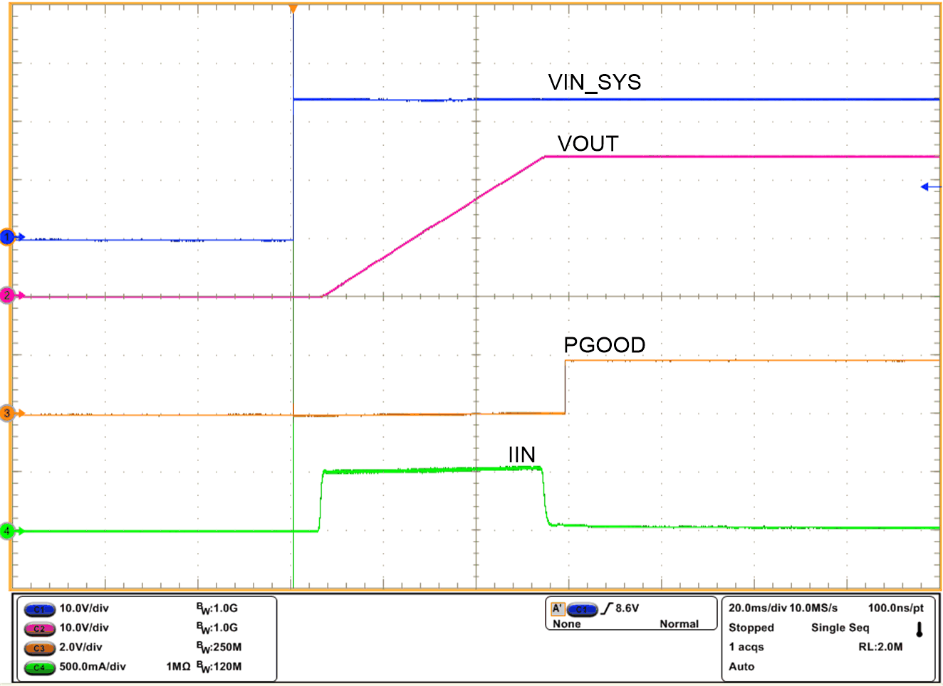
Figure 10-3 Hot-Plug In at 24-V Supply
GUID-443891A0-AE86-4585-92F4-4E713F26E365-low.png
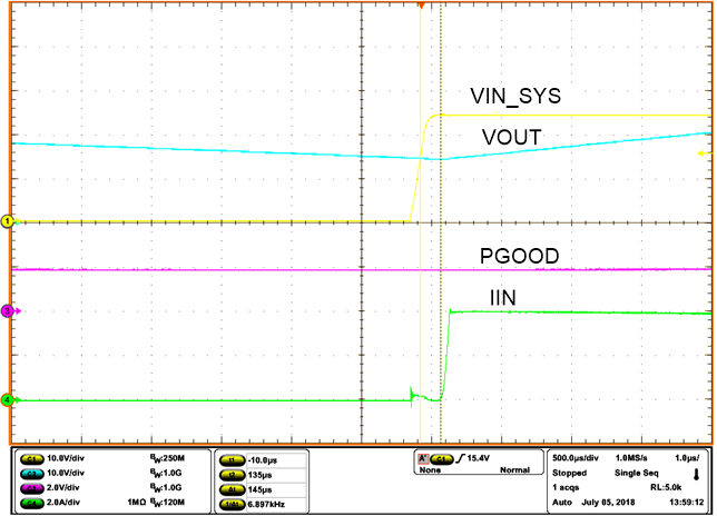
Figure 10-5 Voltage Interruption Response With TPS26630 (Zoomed)
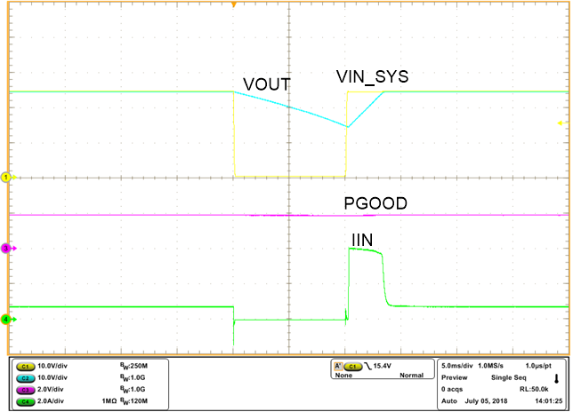
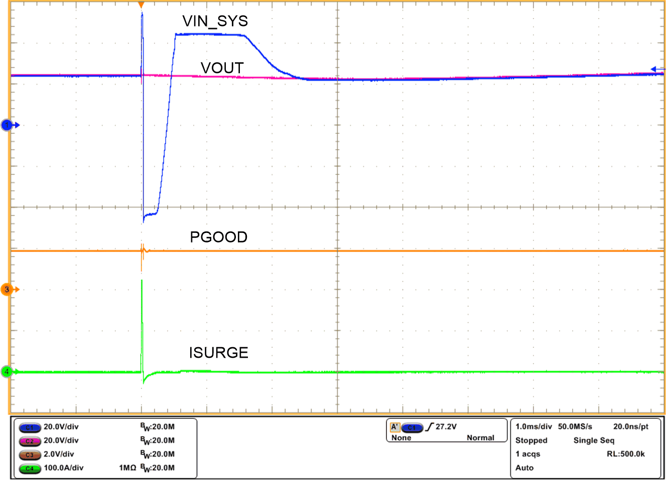
GUID-AE18AA8B-019E-441C-9C13-CDC9F6057889-low.png
Figure 10-7 Voltage Interruption Performance With TPS26631
GUID-031A0116-30AA-440A-9468-0214272E98B1-low.gif
Figure 10-9 500-V, 2-Ω Surge Response
GUID-59944835-479E-4C81-BF8B-9D7163375207-low.png
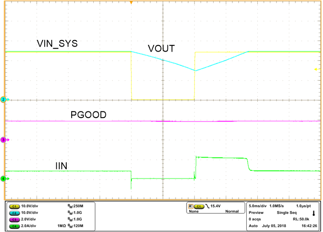
Figure 10-4 Voltage Interruption Response With TPS26630
GUID-53F1D96E-7A10-4207-8151-85E5EBB87738-low.gif
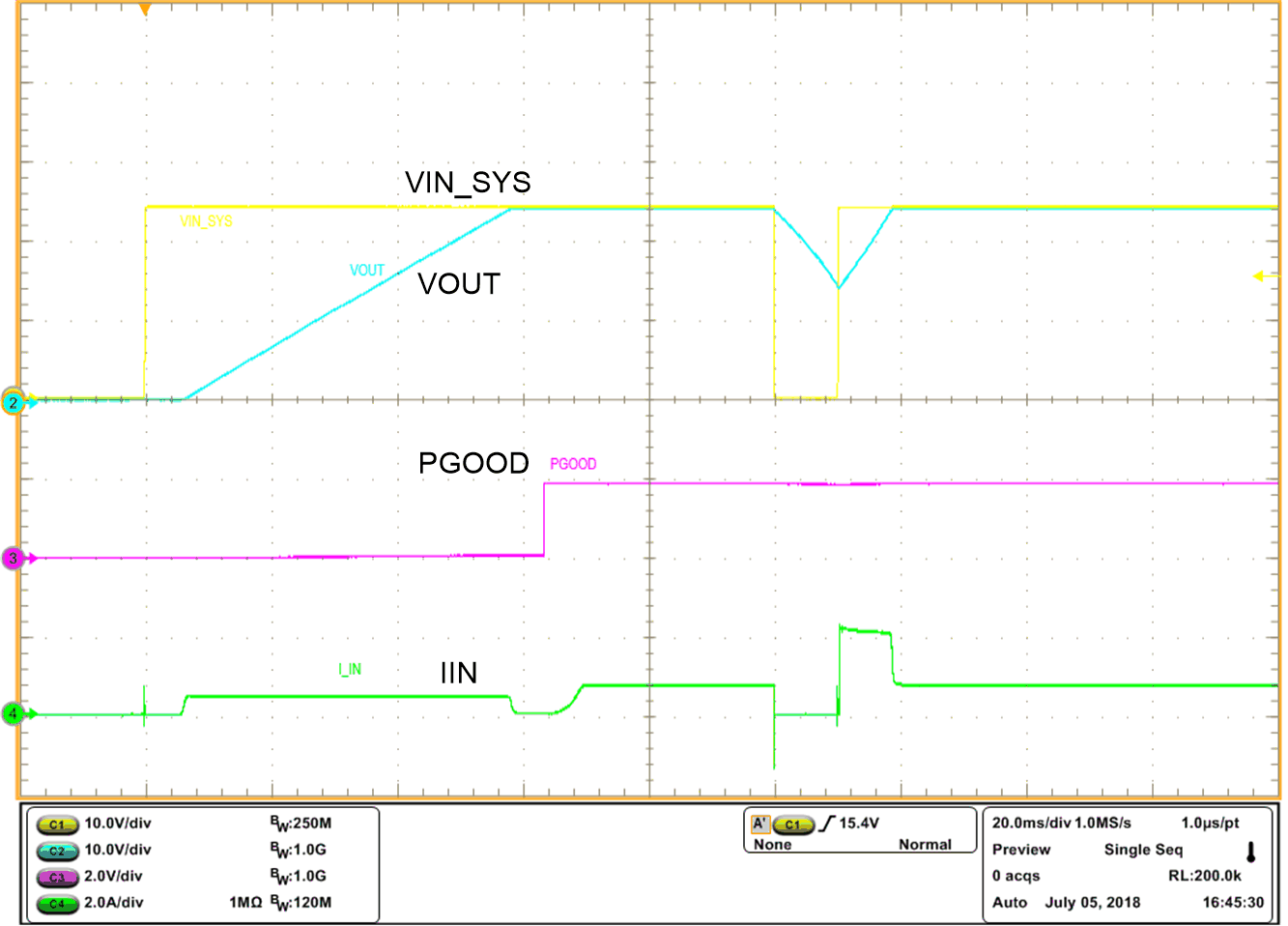
Figure 10-6 Power Up Followed With Voltage Interruption With TPS26630
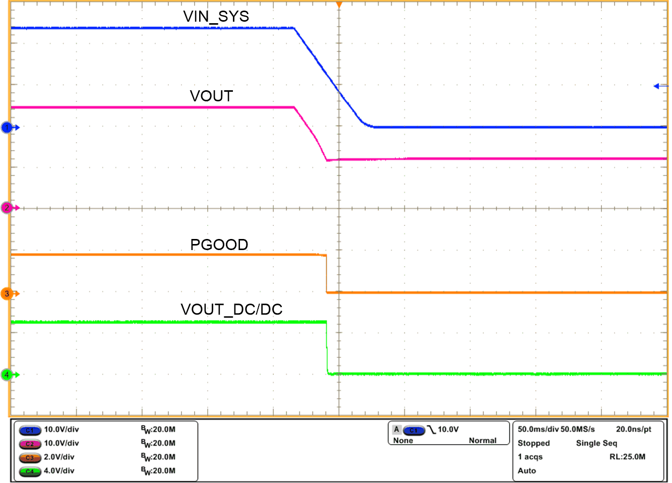
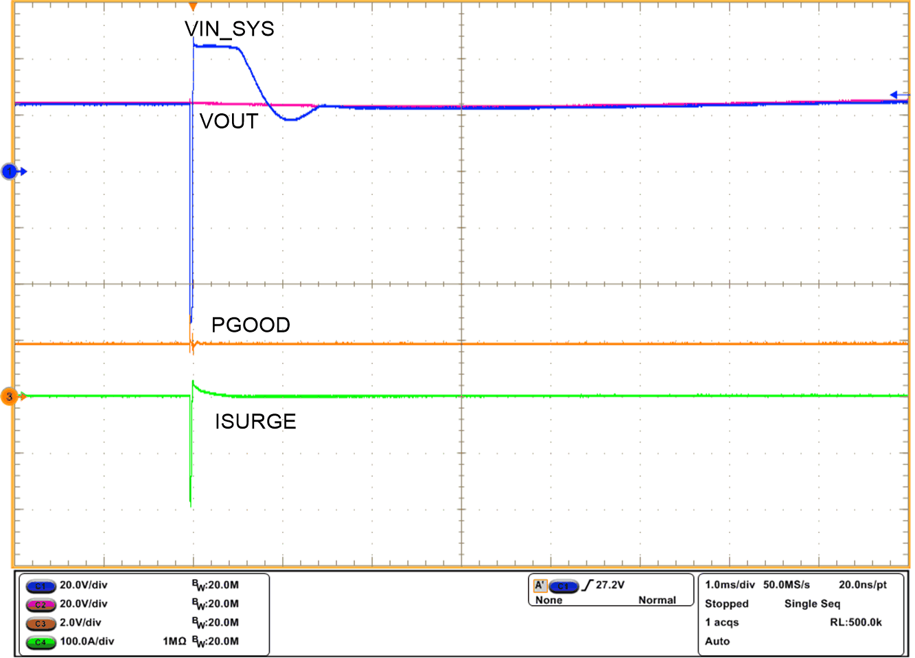
GUID-045D4F18-84BC-4BA8-A1A6-9E460E32DDC3-low.gif
Figure 10-8 Power Down Response
GUID-82F1D664-F16F-41B6-9DCD-3BA4133456F7-low.gif
Figure 10-10 –500-V, 2-Ω Surge Response