JAJSGA2F September 2018 – June 2021 TPS2663
PRODUCTION DATA
- 1 特長
- 2 アプリケーション
- 3 概要
- 4 Revision History
- 5 Device Comparison Table
- 6 Pin Configuration and Functions
- 7 Specifications
- 8 Parameter Measurement Information
-
9 Detailed Description
- 9.1 Overview
- 9.2 Functional Block Diagram
- 9.3
Feature Description
- 9.3.1 Hot Plug-In and In-Rush Current Control
- 9.3.2 PGOOD and PGTH
- 9.3.3 Undervoltage Lockout (UVLO)
- 9.3.4 Overvoltage Protection (OVP)
- 9.3.5 Input Reverse Polarity Protection (B_GATE, DRV)
- 9.3.6 Reverse Current Protection
- 9.3.7 Overload and Short Circuit Protection
- 9.3.8 Output Power Limiting, PLIM (TPS26632, TPS26633, TPS26635 and TPS26636 Only)
- 9.3.9 Current Monitoring Output (IMON)
- 9.3.10 FAULT Response ( FLT)
- 9.3.11 IN_SYS, IN, OUT and GND Pins
- 9.3.12 Thermal Shutdown
- 9.3.13 Low Current Shutdown Control (SHDN)
- 9.4 Device Functional Modes
-
10Application and Implementation
- 10.1 Application Information
- 10.2
Typical Application: Power Path Protection in a PLC System
- 10.2.1 Design Requirements
- 10.2.2 Detailed Design Procedure
- 10.2.3 Application Curves
- 10.3 System Examples
- 10.4 Do's and Don'ts
- 11Power Supply Recommendations
- 12Layout
- 13Device and Documentation Support
- 14Mechanical, Packaging, and Orderable Information
9.3.1.1 Thermal Regulation Loop
The average power dissipation within the eFuse during power up with a capacitive load can be calculated using Equation 3.

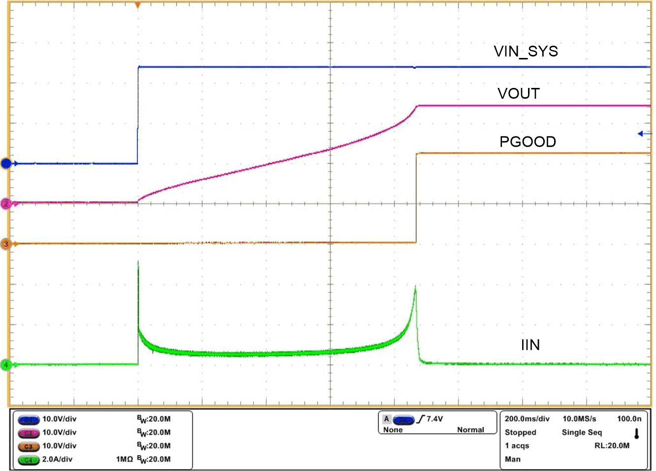
System designs requiring to charge large output capacitors rapidly may result in an operating point that exceeds the power dissipation versus time boundary limits of the device defined by Figure 7-18 characteristic curve. This may result in increase in junction temperature beyond the device's maximum allowed junction temperature. To keep the junction temperature within the operating range, the thermal regulation control loop regulates the junction temperature at T(J_REG), 145°C (typical) by controlling the inrush current profile and thereby limiting the power dissipation within the device automatically. An internal 2.5 seconds (typical) timer starts from the instance the thermal regulation operation kicks in. If the output does not power up within this time then the internal FET is turned OFF. Subsequent operation of the device depends on the MODE configuration (Auto-Retry or latch OFF) setting as shown in Table 9-1. The maximum time-out of 1.25 seconds (typical) in thermal regulation loop operation ensures that the device and the system board does not heat up during steady fault conditions such as wake up with output short-circuit. This scheme ensures reliable power up operation.
Thermal regulation control loop is internally enabled during power up by V(IN), UVLO cycling and turn ON using SHDN control. Figure 8-2 illustrates performance of the device operating in thermal regulation loop during power up by V(IN) with a large output capacitor. The Thermal regulation loop gets disabled internally after the power up sequence when the internal FET's gate gets fully enhanced or when the t(Treg_timeout) of 2.5 seconds (typical) time is elapsed.

| CdVdT = Open | COUT = 30 mF | RILIM = 4.02 kΩ |