JAJSK93 November   2020 TPS27SA08

PRODUCTION DATA  

  1. 特長
  2. アプリケーション
  3. 概要
  4. Revision History
  5. Device Summary Table
  6. Pin Configuration and Functions
    1. 6.1 Recommended Connections for Unused Pins
  7. Specifications
    1. 7.1 Absolute Maximum Ratings
    2. 7.2 ESD Ratings
    3. 7.3 Recommended Operating Conditions
    4. 7.4 Thermal Information
    5. 7.5 Electrical Characteristics
    6. 7.6 Switching Characteristics
    7. 7.7 SNS Timing Characteristics
    8. 7.8 Typical Characteristics
  8. Parameter Measurement Information
  9. Detailed Description
    1. 9.1 Overview
    2. 9.2 Functional Block Diagram
    3. 9.3 Feature Description
      1. 9.3.1 Protection Mechanisms
        1. 9.3.1.1 Thermal Shutdown
        2. 9.3.1.2 Current Limit
          1. 9.3.1.2.1 Current Limit Foldback
          2. 9.3.1.2.2 Undervoltage Lockout (UVLO)
          3. 9.3.1.2.3 VBB during Short-to-Ground
        3. 9.3.1.3 Energy Limit
        4. 9.3.1.4 Voltage Transients
          1. 9.3.1.4.1 Driving Inductive and Capacitive Loads
        5. 9.3.1.5 Reverse supply
        6. 9.3.1.6 Fault Event – Timing Diagrams
      2. 9.3.2 Diagnostic Mechanisms
        1. 9.3.2.1 VOUT Short-to-supply and Open-Load
          1. 9.3.2.1.1 Detection With Switch Enabled
          2. 9.3.2.1.2 Detection With Switch Disabled
        2. 9.3.2.2 SNS Output
          1. 9.3.2.2.1 RSNS Value
            1. 9.3.2.2.1.1 High Accuracy Load Current Sense
            2. 9.3.2.2.1.2 SNS Output Filter
        3. 9.3.2.3 ST Pin
        4. 9.3.2.4 Fault Indication and SNS Mux
        5. 9.3.2.5 Resistor Sharing
        6. 9.3.2.6 High-Frequency, Low Duty-Cycle Current Sensing
    4. 9.4 Device Functional Modes
      1. 9.4.1 Off
      2. 9.4.2 Standby
      3. 9.4.3 Diagnostic
      4. 9.4.4 Standby Delay
      5. 9.4.5 Active
      6. 9.4.6 Fault
  10. 10Application and Implementation
    1. 10.1 Application Information
      1. 10.1.1 Ground Protection Network
      2. 10.1.2 Interface With Microcontroller
      3. 10.1.3 I/O Protection
      4. 10.1.4 Inverse Current
      5. 10.1.5 Loss of GND
      6. 10.1.6 Thermal Information
    2. 10.2 Typical Application
      1. 10.2.1 Design Requirements
      2. 10.2.2 Detailed Design Procedure
        1. 10.2.2.1 Thermal Considerations
        2. 10.2.2.2 Diagnostics
          1. 10.2.2.2.1 Selecting the RISNS Value
      3. 10.2.3 Application Curves
  11. 11Power Supply Recommendations
  12. 12Layout
    1. 12.1 Layout Guidelines
    2. 12.2 Layout Example
  13. 13Device and Documentation Support
    1. 13.1 Device Support
      1. 13.1.1 Related Documentation
    2. 13.2 Trademarks
    3. 13.3 静電気放電に関する注意事項
    4. 13.4 用語集
  14. 14Mechanical, Packaging, and Orderable Information

パッケージ・オプション

メカニカル・データ(パッケージ|ピン)
サーマルパッド・メカニカル・データ
発注情報
Detection With Switch Disabled

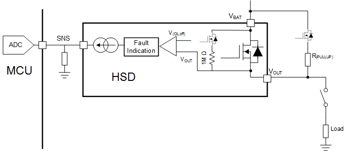
While the switch is disabled, if DIA_EN is high, an internal comparator will detect the condition of VOUT. If the load is disconnected (open load condition) or there is a short to supply theOUT voltage will be higher than the open load threshold (VOL,off) and a fault is indicated on the SNS pin. An internal pull-up of 1 MΩ is in series with an internal MOSFET switch, so no external component is required if only a completely open load needs to be detected. However, if there is significant leakage or other current draw even when the load is disconnected, a lower value pull-up resistor and switch can be added externally to set the VOUT voltage above the VOL,off during open load conditions.
GUID-2660BAB2-B8BB-4EFD-BFAF-0125058E46BF-low.gif
This figure assumes that the device ground and the load ground are at the same potential. In application, there may be a ground shift voltage of 1 V to 2 V.
Figure 9-7 Short to supply and Open Load Detection

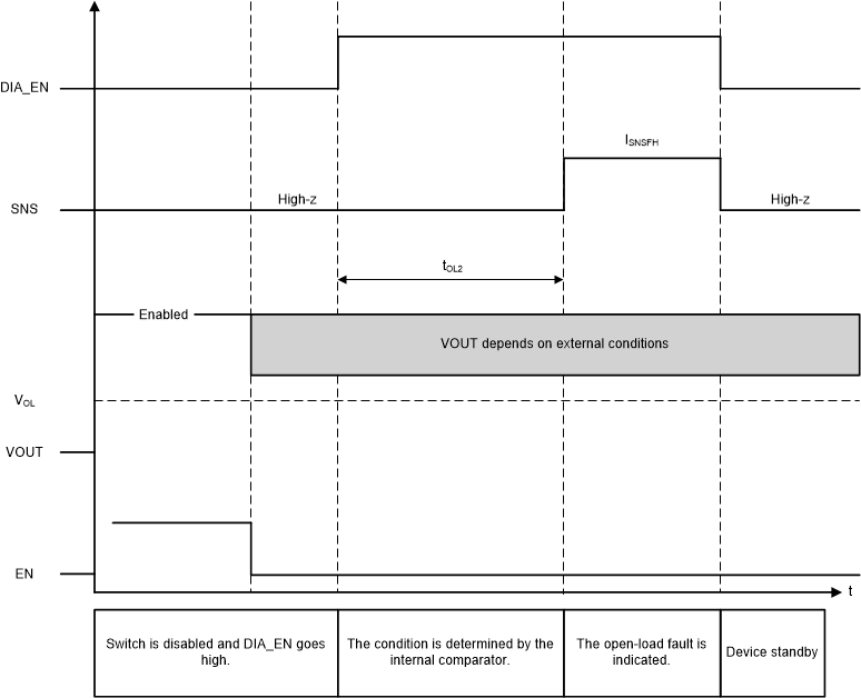
The detection circuitry is only enabled when DIA_EN = HIGH and EN = LOW.

If VOUT > VOL, the SNS pin will go to the fault level.

If VOUT < VOL, then there is no fault indication.

The fault indication will only occur if the SEL1 pin is set to diagnose the channel.

While the switch is disabled and DIA_EN is high, the fault indication mechanisms will continuously represent the present status. For example, if VOUT decreases from >VOL to <VOL, the fault indication is reset. Additionally, the fault indication is reset upon the falling edge of DIA_EN or the rising edge of EN.
GUID-6FF135FD-7E43-4045-B5BE-A3AD86F84246-low.gif Figure 9-8 Open Load