JAJSM08B December 2022 – August 2024 TPS281C30
PRODUCTION DATA
- 1
- 1 特長
- 2 アプリケーション
- 3 概要
- 4 Device Comparison Table
- 5 Pin Configuration and Functions
- 6 Specifications
- 7 Parameter Measurement Information
-
8 Detailed Description
- 8.1 Overview
- 8.2 Functional Block Diagram
- 8.3 Device Functional Modes
- 8.4
Feature Description
- 8.4.1 Accurate Current Sense
- 8.4.2 Programmable Current Limit
- 8.4.3 Inductive-Load Switching-Off Clamp
- 8.4.4 Inductive Load Demagnetization
- 8.4.5
Full Protections and Diagnostics
- 8.4.5.1 Open-Load Detection
- 8.4.5.2 Thermal Protection Behavior
- 8.4.5.3 Undervoltage Lockout (UVLO) Protection
- 8.4.5.4 Overvoltage (OVP) Protection
- 8.4.5.5 Reverse Polarity Protection
- 8.4.5.6 Protection for MCU I/Os
- 8.4.5.7 Diagnostic Enable Function
- 8.4.5.8 Loss of Ground
- 8.4.5.9 Enhanced EFT Immunity
- 9 Application and Implementation
- 10Device and Documentation Support
- 11Revision History
- 12Mechanical, Packaging, and Orderable Information
パッケージ・オプション
メカニカル・データ(パッケージ|ピン)
- RGW|20
サーマルパッド・メカニカル・データ
- RGW|20
発注情報
8.4.4 Inductive Load Demagnetization
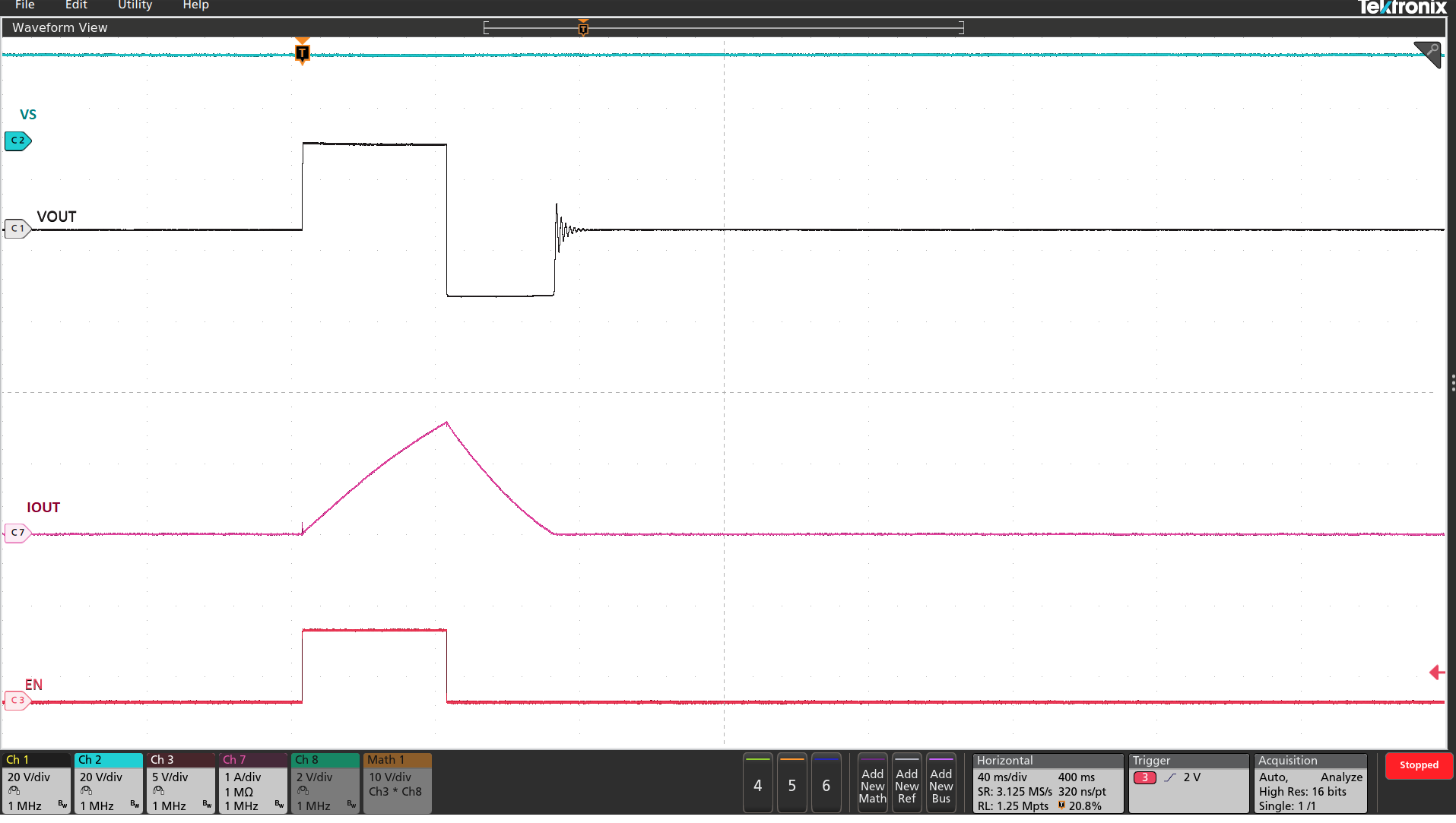
When switching off an inductive load, the inductor can impose a negative voltage on the output of the switch. The TPS281C30 includes voltage clamps between VS and VOUT to limit the voltage across the FETs and demagnetize load inductance if there is any. The negative voltage applied at the OUT pin drives the discharge of inductor current. Figure 8-13 shows the device discharging a 400-mH load.
 Figure 8-13 TPS281C30 Inductive Discharge
(400 mH)
Figure 8-13 TPS281C30 Inductive Discharge
(400 mH)The maximum acceptable load inductance is a function of the energy dissipated in the device and therefore the load current and the inductive load. The maximum energy and the load inductance the device can withstand for one pulse inductive dissipation at 125°C is shown in Figure 8-14. The device (version A, B) can withstand 40% of this energy for one million inductive repetitive pulses with a >4-Hz repetitive pulse. If the application parameters exceed this device limit, use a protection device like a freewheeling diode to dissipate the energy stored in the inductor.
 Figure 8-14 TPS281C30 Inductive Load
Discharge Energy Capability at 125°C