JAJSC54E May   2006  – January 2024 TPS28225

PRODUCTION DATA  

  1.   1
  2. 特長
  3. アプリケーション
  4. 概要
  5. Pin Configuration and Functions
  6. Specifications
    1. 5.1 Absolute Maximum Ratings
    2. 5.2 ESD Ratings
    3. 5.3 Recommended Operating Conditions
    4. 5.4 Thermal Information
    5. 5.5 Electrical Characteristics
    6. 5.6 Switching Characteristics
    7. 5.7 Typical Characteristics
  7. Detailed Description
    1. 6.1 Overview
    2. 6.2 Functional Block Diagram
    3. 6.3 Feature Description
      1. 6.3.1 Undervoltage Lockout (UVLO)
      2. 6.3.2 Output Active Low
      3. 6.3.3 Enable/Power Good
      4. 6.3.4 3-State Input
        1. 6.3.4.1 TPS28225 3-State Exit Mode
        2. 6.3.4.2 External Resistor Interference
      5. 6.3.5 Bootstrap Diode
      6. 6.3.6 Upper and Lower Gate Drivers
      7. 6.3.7 Dead-Time Control
      8. 6.3.8 Thermal Shutdown
    4. 6.4 Device Functional Modes
  8. Application and Implementation
    1. 7.1 Application Information
    2. 7.2 Typical Application
      1. 7.2.1 Design Requirements
      2. 7.2.2 Detailed Design Procedure
        1. 7.2.2.1 Four Phases Driven by TPS28225 Driver
        2. 7.2.2.2 Switching The MOSFETs
        3. 7.2.2.3 List of Materials
      3. 7.2.3 Application Curves
    3. 7.3 System Examples
  9. Power Supply Recommendations
  10. Layout
    1. 9.1 Layout Guidelines
    2. 9.2 Layout Example
  11. 10Device and Documentation Support
    1. 10.1 Device Support
      1. 10.1.1 サード・パーティ製品に関する免責事項
    2. 10.2 Documentation Support
      1. 10.2.1 Related Documentation
    3. 10.3 ドキュメントの更新通知を受け取る方法
    4. 10.4 サポート・リソース
    5. 10.5 Trademarks
    6. 10.6 静電気放電に関する注意事項
    7. 10.7 用語集
  12. 11Revision History
  13. 12Mechanical, Packaging, and Orderable Information

パッケージ・オプション

メカニカル・データ(パッケージ|ピン)
サーマルパッド・メカニカル・データ
発注情報

Typical Application

The DC-DC converter in Figure 7-1 displays the schematic of the TPS28225 in a multiphase high-current step-down power supply (only one phase is shown). This design uses a single high-side MOSFET Q10 and two low-side MOSFETs Q8 and Q9, the latter connected in parallel. The TPS28225 is controlled by multiphase buck DC-to-DC controller like TPS40090. As TPS28225 has internal shoot-through protection only one PWM control signal is required for each channel.
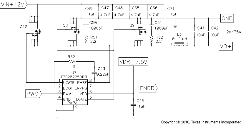
GUID-E5F16D16-0BA1-4B00-8BE3-78B609827B8F-low.gif Figure 7-1 One of Four Phases Driven by TPS28225 Driver in 4-Phase VRM Reference Design