JAJSC54E May 2006 – January 2024 TPS28225
PRODUCTION DATA
- 1
- 1 特長
- 2 アプリケーション
- 3 概要
- 4 Pin Configuration and Functions
- 5 Specifications
- 6 Detailed Description
- 7 Application and Implementation
- 8 Power Supply Recommendations
- 9 Layout
- 10Device and Documentation Support
- 11Revision History
- 12Mechanical, Packaging, and Orderable Information
パッケージ・オプション
メカニカル・データ(パッケージ|ピン)
サーマルパッド・メカニカル・データ
- DRB|8
発注情報
6.3.4.2 External Resistor Interference
Any external resistor between PWM input and GND with the value lower than 40 kΩ can interfere with the 3-state thresholds. If the driver is intended to operate in the 3-state mode, any resistor below 40 kΩ at the PWM and GND should be avoided. A resistor lower than 3.5 kΩ connected between the PWM and GND completely disables the 3-state function. In such case, the 3-state window shrinks to zero and the lower 3-state threshold becomes the boundary between the UGATE staying low and LGATE being high and vice versa depending on the PWM input signal applied. It is not necessary to use a resistor <3.5 kΩ to avoid the 3-state condition while using a controller that is 3-state capable. If the rise and fall time of the input PWM signal is shorter than 250 ns, then the driver never enters into the 3-state mode.
In the case where the low-side MOSFET of a buck converter stays on during shutdown, the 3-state feature can be fused to avoid negative resonant voltage across the output capacitor. This feature also can be used during start up with a pre-biased output in the case where pulling the output low during the startup is not allowed due to system requirements. If the system controller does not have the 3-state feature and never goes into the high-impedance state, then setting the EN/PG signal low will keep both gate drive outputs low and turn both low- and high-side MOSFETs OFF during the shut down and start up with the pre-biased output.
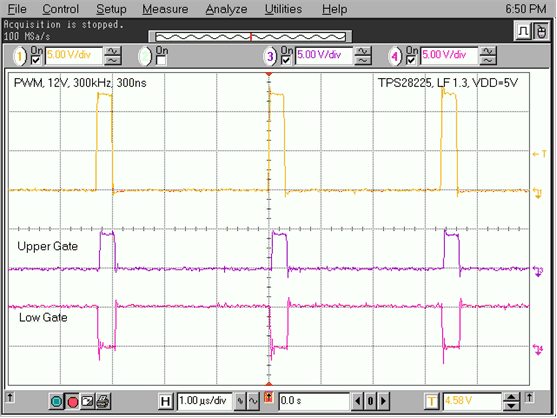
The self-adjustable input circuit accepts wide range of input pulse amplitudes (2 V up to 13.2 V) allowing use of a variety of controllers with different outputs including logic level. The wide PWM input voltage allows some flexibility if the driver is used in secondary side synchronous rectifier circuit. The operation of the TPS28225 with a 12-V input PWM pulse amplitude, and with VDD = 7.2 V and VDD = 5 V respectively is shown in Figure 6-4 and Figure 6-5.
 Figure 6-4 12-V PWM Pulse at VDD = 7.2 V
 Figure 6-5 12-V PWM Pulse at VDD = 5 V