JAJSC54E May 2006 – January 2024 TPS28225
PRODUCTION DATA
- 1
- 1 特長
- 2 アプリケーション
- 3 概要
- 4 Pin Configuration and Functions
- 5 Specifications
- 6 Detailed Description
- 7 Application and Implementation
- 8 Power Supply Recommendations
- 9 Layout
- 10Device and Documentation Support
- 11Revision History
- 12Mechanical, Packaging, and Orderable Information
パッケージ・オプション
メカニカル・データ(パッケージ|ピン)
サーマルパッド・メカニカル・データ
- DRB|8
発注情報
7.2.2.2 Switching The MOSFETs
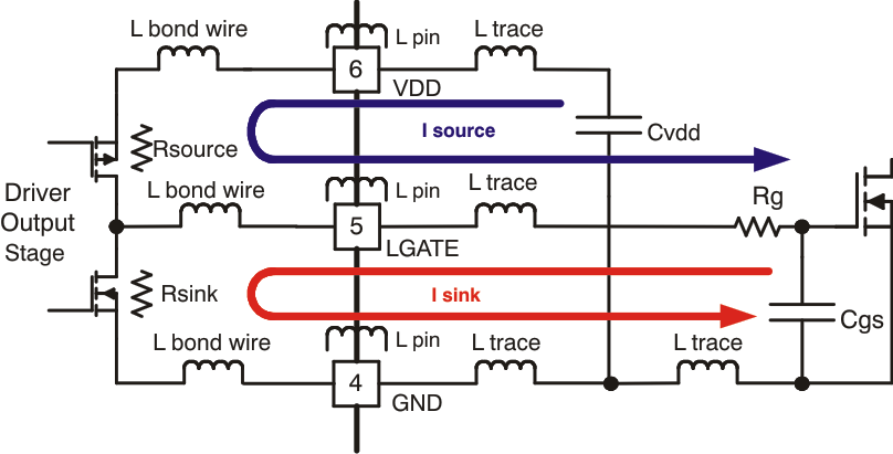
Driving the MOSFETs efficiently at high switching frequencies requires special attention to layout and the reduction of parasitic inductances. Efforts need to be done both at the driver’s die and package level and at the PCB layout level to keep the parasitic inductances as low as possible. Figure 7-4 shows the main parasitic inductances and current flow during turning ON and OFF of the MOSFET by charging its CGS gate capacitance.
 Figure 7-4 MOSFET Drive Paths and Main Circuit Parasitics
The ISOURCE current charges the gate capacitor and the ISINK current discharges it. The rise and fall time of voltage across the gate defines how quickly the MOSFET can be switched. The timing parameters specified in datasheet for both upper and lower driver are shown in Figure 5-16 and Figure 5-17 where 3-nF load capacitor has been used for the characterization data. Based on these actual measurements, the analytical curves in Figure 7-5 and Figure 7-6 show the output voltage and current of upper and low side drivers during the discharging of load capacitor. The left waveforms show the voltage and current as a function of time, while the right waveforms show the relation between the voltage and current during fast switching. These waveforms show the actual switching process and its limitations because of parasitic inductances. The static VOUT/ IOUT curves shown in many datasheets and specifications for the MOSFET drivers do not replicate actual switching condition and provide limited information for the user.
Turning Off of the MOSFET needs to be done as fast as possible to reduce switching losses. For this reason the TPS28225 driver has very low output impedance specified as 0.4 Ω typical for lower driver and 1 Ω typical for upper driver at DC current. Assuming 8-V drive voltage and no parasitic inductances, one can expect an initial sink current amplitude of 20 A and 8 A respectively for the lower and upper drivers. With pure R-C discharge circuit for the gate capacitor, the voltage and current waveforms are expected to be exponential. However, because of parasitic inductances, the actual waveforms have some ringing and the peak current for the lower driver is about 4 A and about 2.5 A for the upper driver (Figure 7-5 and Figure 7-6). The overall parasitic inductance for the lower drive path is estimated as 4 nH and for the upper drive path as 6 nH. The internal parasitic inductance of the driver, which includes inductances of bonded wires and package leads, can be estimated for SOIC-8 package as 2 nH for lower gate and 4 nH for the upper gate. Use of DFN-8 package reduces the internal parasitic inductances by approximately 50%.
 Figure 7-5 LGATE Turning Off Voltage and Sink Current vs Time (Related Switching Diagram (right))
 Figure 7-6 UGATE Turning Off Voltage and Sink Current vs Time (Related Switching Diagram (right))