JAJSEZ1D December   2015  – December 2019 TPS2H000-Q1

PRODUCTION DATA.  

  1. 特長
  2. アプリケーション
  3. 概要
    1.     Device Images
      1.      代表的なアプリケーションの回路図
      2.      可変電流制限による容量性負荷の駆動
  4. 改訂履歴
  5. Device Comparison Table
  6. Pin Configuration and Functions
    1.     Pin Functions
  7. Specifications
    1. 7.1 Absolute Maximum Ratings
    2. 7.2 ESD Ratings
    3. 7.3 Recommended Operating Conditions
    4. 7.4 Thermal Information
    5. 7.5 Electrical Characteristics
    6. 7.6 Switching Characteristics
    7. 7.7 Typical Characteristics
  8. Detailed Description
    1. 8.1 Overview
    2. 8.2 Functional Block Diagram
    3. 8.3 Feature Description
      1. 8.3.1 Pin Current and Voltage Conventions
      2. 8.3.2 Accurate Current Sense
      3. 8.3.3 Adjustable Current Limit
      4. 8.3.4 Inductive-Load Switching-Off Clamp
      5. 8.3.5 Fault Detection and Reporting
        1. 8.3.5.1 Diagnostic Enable Function
        2. 8.3.5.2 Multiplexing of Current Sense
        3. 8.3.5.3 Fault Table
        4. 8.3.5.4 STx and FAULT Reporting
      6. 8.3.6 Full Diagnostics
        1. 8.3.6.1 Short-to-GND and Overload Detection
        2. 8.3.6.2 Open-Load Detection
          1. 8.3.6.2.1 Channel On
          2. 8.3.6.2.2 Channel Off
        3. 8.3.6.3 Short-to-Battery Detection
        4. 8.3.6.4 Reverse Polarity Detection
        5. 8.3.6.5 Thermal Fault Detection
          1. 8.3.6.5.1 Thermal Shutdown
      7. 8.3.7 Full Protections
        1. 8.3.7.1 UVLO Protection
        2. 8.3.7.2 Loss-of-GND Protection
        3. 8.3.7.3 Protection for Loss of Power Supply
        4. 8.3.7.4 Reverse-Current Protection
        5. 8.3.7.5 MCU I/O Protection
    4. 8.4 Device Functional Modes
      1. 8.4.1 Working Modes
  9. Application and Implementation
    1. 9.1 Application Information
    2. 9.2 Typical Application
      1. 9.2.1 Design Requirements
      2. 9.2.2 Detailed Design Procedure
      3. 9.2.3 Application Curves
  10. 10Power Supply Recommendations
  11. 11Layout
    1. 11.1 Layout Guidelines
    2. 11.2 Layout Examples
      1. 11.2.1 Without a GND Network
      2. 11.2.2 With a GND Network
  12. 12デバイスおよびドキュメントのサポート
    1. 12.1 ドキュメントの更新通知を受け取る方法
    2. 12.2 コミュニティ・リソース
    3. 12.3 商標
    4. 12.4 静電気放電に関する注意事項
    5. 12.5 Glossary
  13. 13メカニカル、パッケージ、および注文情報

パッケージ・オプション

メカニカル・データ(パッケージ|ピン)
サーマルパッド・メカニカル・データ
発注情報

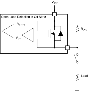
Channel Off

When a channel is off, if a load is connected, the output is pulled down to GND. But if an open load occurs, the output voltage is close to the supply voltage (VVS – VOUTx < V(ol,off)), and the fault is reported out.

There is always a leakage current I(ol,off) present on the output due to internal logic control path or external humidity, corrosion, and so forth. Thus, TI recommends an external pullup resistor to offset the leakage current when an open load is detected. The recommended pullup resistance is 20 kΩ.
TPS2H000-Q1 open-load-det_SLVSCV8.gifFigure 32. Open-Load Detection in Off-State