JAJSES3D December   2015  – December 2019 TPS2H160-Q1

PRODUCTION DATA.  

  1. 特長
  2. アプリケーション
  3. 概要
    1.     Device Images
      1.      代表的なアプリケーションの回路図
      2.      可変電流制限による容量性負荷の駆動
  4. 改訂履歴
  5. Device Comparison Table
  6. Pin Configuration and Functions
    1.     Pin Functions
  7. Specifications
    1. 7.1 Absolute Maximum Ratings
    2. 7.2 ESD Ratings
    3. 7.3 Recommended Operating Conditions
    4. 7.4 Thermal Information
    5. 7.5 Electrical Characteristics
    6. 7.6 Switching Characteristics
    7. 7.7 Typical Characteristics
  8. Detailed Description
    1. 8.1 Overview
    2. 8.2 Functional Block Diagram
    3. 8.3 Feature Description
      1. 8.3.1 Pin Current and Voltage Conventions
      2. 8.3.2 Accurate Current Sense
      3. 8.3.3 Adjustable Current Limit
      4. 8.3.4 Inductive-Load Switching-Off Clamp
      5. 8.3.5 Fault Detection and Reporting
        1. 8.3.5.1 Diagnostic Enable Function
        2. 8.3.5.2 Multiplexing of Current Sense
        3. 8.3.5.3 Fault Table
        4. 8.3.5.4 STx and FAULT Reporting
      6. 8.3.6 Full Diagnostics
        1. 8.3.6.1 Short-to-GND and Overload Detection
        2. 8.3.6.2 Open-Load Detection
          1. 8.3.6.2.1 Channel On
          2. 8.3.6.2.2 Channel Off
        3. 8.3.6.3 Short-to-Battery Detection
        4. 8.3.6.4 Reverse Polarity Detection
        5. 8.3.6.5 Thermal Fault Detection
          1. 8.3.6.5.1 Thermal Shutdown
      7. 8.3.7 Full Protections
        1. 8.3.7.1 UVLO Protection
        2. 8.3.7.2 Loss-of-GND Protection
        3. 8.3.7.3 Protection for Loss of Power Supply
        4. 8.3.7.4 Reverse-Current Protection
        5. 8.3.7.5 MCU I/O Protection
    4. 8.4 Device Functional Modes
      1. 8.4.1 Working Modes
  9. Application and Implementation
    1. 9.1 Application Information
    2. 9.2 Typical Application
      1. 9.2.1 Design Requirements
      2. 9.2.2 Detailed Design Procedure
      3. 9.2.3 Application Curves
  10. 10Power Supply Recommendations
  11. 11Layout
    1. 11.1 Layout Guidelines
    2. 11.2 Layout Examples
      1. 11.2.1 Without a GND Network
      2. 11.2.2 With a GND Network
  12. 12デバイスおよびドキュメントのサポート
    1. 12.1 ドキュメントの更新通知を受け取る方法
    2. 12.2 コミュニティ・リソース
    3. 12.3 商標
    4. 12.4 静電気放電に関する注意事項
    5. 12.5 Glossary
  13. 13メカニカル、パッケージ、および注文情報

パッケージ・オプション

メカニカル・データ(パッケージ|ピン)
サーマルパッド・メカニカル・データ
発注情報

Accurate Current Sense

High-accuracy current sense is implemented in the version-B device. It allows a better real-time monitoring effect and more-accurate diagnostics without further calibration.

One integrated current mirror can source 1 / K(CS) of the load current, and the mirrored current flows into the external current sense resistor to become a voltage signal. The current mirror is shared by the four channels. K(CS) is the ratio of the output current and the sense current. It is a constant value across the temperature and supply voltage. Each device is calibrated accurately during production, so post-calibration is not required. See Figure 23 for more details.
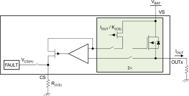
TPS2H160-Q1 CS-blk-dgrm_SLVSD74.gifFigure 23. Current-Sense Block Diagram

When a fault occurs, the CS pin also works as a fault report with a pullup voltage, VCS(H). See Figure 24 for more details.
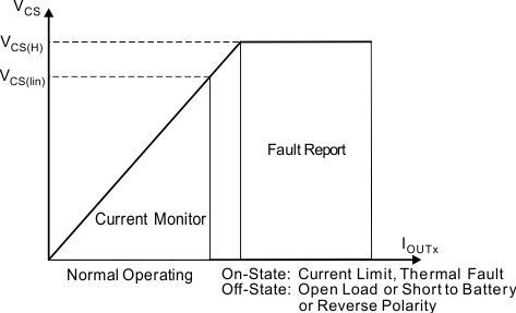
TPS2H160-Q1 CS-voltage-out_SLVSCV8.gifFigure 24. Current-Sense Output-Voltage Curve

Use Equation 1 to calculate R(CS).

Equation 1. TPS2H160-Q1 eq01-Rcs_SLVSCV8.gif

Take the following points into consideration when calculating R(CS).

  • Ensure VCS is within the current-sense linear region (VCS, IOUTx(lin)) across the full range of the load current. Check R(CS) with Equation 2.
  • Equation 2. TPS2H160-Q1 eq02-Rcs-lin_SLVSCV8.gif
  • In fault mode, ensure ICS is within the source capacity of the CS pin (ICS(H)). Check R(CS) with Equation 3.
  • Equation 3. TPS2H160-Q1 eq03-Rcs-fault_SLVSCV8.gif