JAJSLC2C march   2014  – march 2021 TPS3700-Q1

PRODUCTION DATA  

  1.   1
  2. 特長
  3. アプリケーション
  4. 概要
  5. Revision History
  6. Pin Configuration and Functions
  7. Specifications
    1. 6.1 Absolute Maximum Ratings
    2. 6.2 ESD Ratings
    3. 6.3 Recommended Operating Conditions
    4. 6.4 Thermal Information
    5. 6.5 Electrical Characteristics
    6. 6.6 Timing Requirements
    7. 6.7 Timing Diagram
    8. 6.8 Switching Characteristics
    9. 6.9 Typical Characteristics
  8. Detailed Description
    1. 7.1 Overview
    2. 7.2 Functional Block Diagram
    3. 7.3 Feature Description
      1. 7.3.1 Inputs (INA+, INB–)
      2. 7.3.2 Outputs (OUTA, OUTB)
      3. 7.3.3 Window Voltage Detector
      4. 7.3.4 Immunity to Input Terminal Voltage Transients
    4. 7.4 Device Functional Modes
  9. Application and Implementation
    1. 8.1 Application Information
      1. 8.1.1 VPULLUP to a Voltage Other Than VDD
      2. 8.1.2 Monitoring VDD
      3. 8.1.3 Monitoring a Voltage Other Than VDD
      4. 8.1.4 Monitoring Overvoltage and Undervoltage for Separate Rails
    2. 8.2 Typical Application
      1. 8.2.1 Design Requirements
        1. 8.2.1.1 Input Supply Capacitor
        2. 8.2.1.2 Input Capacitors
      2. 8.2.2 Detailed Design Procedure
      3. 8.2.3 Application Curves
  10. Power Supply Recommendations
  11. 10Layout
    1. 10.1 Layout Guidelines
    2. 10.2 Layout Example
  12. 11Device and Documentation Support
    1. 11.1 Documentation Support
      1. 11.1.1 Related Documentation
    2. 11.2 Trademarks
    3. 11.3 静電気放電に関する注意事項
    4. 11.4 用語集
  13. 12Mechanical, Packaging, and Orderable Information

パッケージ・オプション

メカニカル・データ(パッケージ|ピン)
サーマルパッド・メカニカル・データ
発注情報

Typical Characteristics

At TJ = 25°C and VDD = 5 V, unless otherwise noted.
GUID-AE56AFFE-936F-4AC1-B61F-1B9D4EFE5912-low.gif
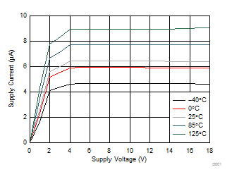
Figure 6-2 Supply Current (IDD) vs Supply Voltage (VDD)
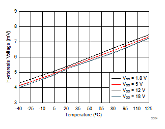
GUID-558DDB22-2651-4861-8E87-5BB615765287-low.gifFigure 6-4 Hysteresis (Vhys) vs Temperature
GUID-E08D653D-C9E8-4A15-AE87-79A280E09075-low.gif
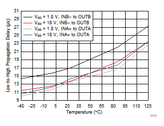
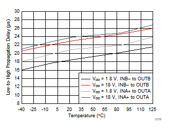
Figure 6-6 Propagation Delay vs Temperature (Low-to-High Transition at the Inputs)
GUID-65BA086C-025A-4731-AEC7-44508ED1FC1D-low.gif
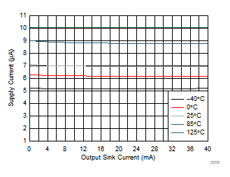
Figure 6-8 Supply Current (IDD) vs Output Sink Current
GUID-ED856DB7-EDC4-423A-A957-F4BF602EDF72-low.gif
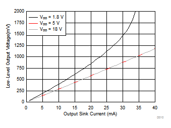
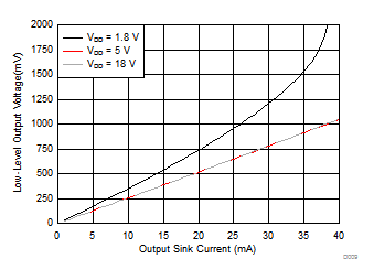
Figure 6-10 Output Voltage Low (VOL) vs Output Sink Current (0°C)
GUID-6629B3DA-CE5E-411A-949D-4BCDD296DAA6-low.gif
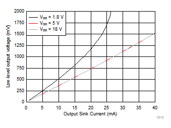
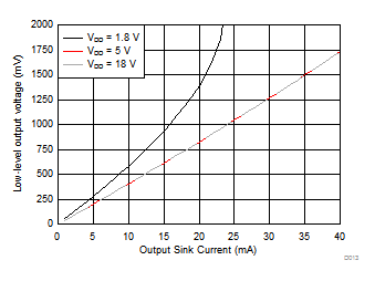
Figure 6-12 Output Voltage Low (VOL) vs Output Sink Current (85°C)
GUID-AE0C1502-8B9A-46EE-B589-15A51AE16FAA-low.gif
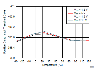
Figure 6-3 Rising Input Threshold Voltage (VIT+) vs Temperature
GUID-3775BC09-9DC8-472A-A150-EC49A740E6DE-low.gifFigure 6-5 Propagation Delay vs Temperature (High-to-Low Transition at the Inputs)
GUID-5C2689F4-CF79-48C5-988D-DBA51EE8EB4D-low.gif
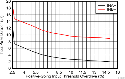
INA+ = negative spike below VIT–
INB– = positive spike above VIT+
Figure 6-7 Minimum Pulse Width vs Threshold Overdrive Voltage
GUID-21A2AB55-3284-4923-B2DB-B00DABA09024-low.gif
Figure 6-9 Output Voltage Low (VOL) vs Output Sink Current (–40°C)
GUID-AA76A2F6-4E07-4801-80C7-09AE7F662BE6-low.gif
Figure 6-11 Output Voltage Low (VOL) vs Output Sink Current (25°C)
GUID-769FD8A1-4D1F-4B14-A1E0-1FA8FE14A04E-low.gif
Figure 6-13 Output Voltage Low (VOL) vs Output Sink Current (125°C)