JAJSFN5C November 2014 – February 2019 TPS3701
PRODUCTION DATA.
8.1.1 Window Voltage Detector Considerations
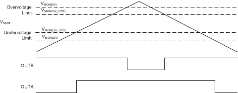
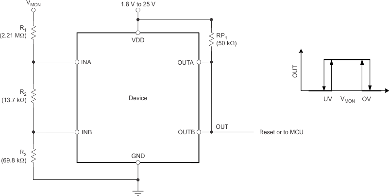
The inverting and noninverting configuration of the comparators forms a window voltage detector circuit using a resistor divider network, as shown in Figure 19 and Figure 20. The input pins can monitor any system voltage above 400 mV with the use of a resistor divider network. INA and INB monitor for undervoltage and overvoltage conditions, respectively.
 Figure 20. Window Voltage Detector Timing Diagram
 The TPS3701 flags the overvoltage or undervoltage condition with the greatest accuracy. The highest accuracy threshold voltages are VIT–(INA) and VIT+(INB), and correspond with the falling undervoltage flag, and the rising overvoltage flag, respectively. These thresholds represent the accuracy when the monitored voltage is within the valid window (both OUTA and OUTB are in a high-impedance state), and correspond to the VMON(UV) and VMON(OV) trigger voltages, respectively. If the monitored voltage is outside of the valid window (VMON is less than the undervoltage limit, VMON(UV), or greater than overvoltage limit, VMON(OV)), then the input threshold voltages to re-enter the valid window are VIT+(INA) or VIT–(INB), and correspond with the VMON(UV_HYS) and VMON(OV_HYS) monitored voltages, respectively.
The resistor divider values and target threshold voltage can be calculated by using Equation 1 through Equation 4:
Choose an RTOTAL value so that the current through the divider is approximately 100 times higher than the input current at the INA and INB pins. Resistors with high values minimize current consumption; however, the input bias current degrades accuracy if the current through the resistors is too low. See application report SLVA450, Optimizing Resistor Dividers at a Comparator Input (SLVA450), for details on sizing input resistors.
R3 is determined by Equation 2:

where
- VMON(OV) is the target voltage at which an overvoltage condition is detected.
R2 is determined by either Equation 3 or Equation 4:

where
- VMON(UV_HYS) is the target voltage at which an undervoltage condition is removed as VMON rises.

where
- VMON(UV) is the target voltage at which an undervoltage condition is detected.
