JAJSFN5C November   2014  – February 2019 TPS3701

PRODUCTION DATA.  

  1. 特長
  2. アプリケーション
  3. 概要
    1.     Device Images
      1.      代表的なアプリケーション
      2.      標準的な誤差と接合部温度との関係
  4. 改訂履歴
  5. Pin Configuration and Functions
    1.     Pin Functions
  6. Specifications
    1. 6.1 Absolute Maximum Ratings
    2. 6.2 ESD Ratings
    3. 6.3 Recommended Operating Conditions
    4. 6.4 Thermal Information
    5. 6.5 Electrical Characteristics
    6. 6.6 Timing Requirements
    7. 6.7 Typical Characteristics
  7. Detailed Description
    1. 7.1 Overview
    2. 7.2 Functional Block Diagram
    3. 7.3 Feature Description
      1. 7.3.1 Inputs (INA, INB)
      2. 7.3.2 Outputs (OUTA, OUTB)
    4. 7.4 Device Functional Modes
      1. 7.4.1 Normal Operation (VDD > UVLO)
      2. 7.4.2 Undervoltage Lockout (V(POR) < VDD < UVLO)
      3. 7.4.3 Power-On-Reset (VDD < V(POR))
  8. Application and Implementation
    1. 8.1 Application Information
      1. 8.1.1 Window Voltage Detector Considerations
      2. 8.1.2 Input and Output Configurations
      3. 8.1.3 Immunity to Input Pin Voltage Transients
    2. 8.2 Typical Application
      1. 8.2.1 Design Requirements
      2. 8.2.2 Detailed Design Procedure
      3. 8.2.3 Application Curve
  9. Power Supply Recommendations
  10. 10Layout
    1. 10.1 Layout Guidelines
    2. 10.2 Layout Example
  11. 11デバイスおよびドキュメントのサポート
    1. 11.1 ドキュメントのサポート
      1. 11.1.1 関連資料
    2. 11.2 ドキュメントの更新通知を受け取る方法
    3. 11.3 コミュニティ・リソース
    4. 11.4 商標
    5. 11.5 静電気放電に関する注意事項
    6. 11.6 Glossary
  12. 12メカニカル、パッケージ、および注文情報

パッケージ・オプション

メカニカル・データ(パッケージ|ピン)
サーマルパッド・メカニカル・データ
発注情報

Input and Output Configurations

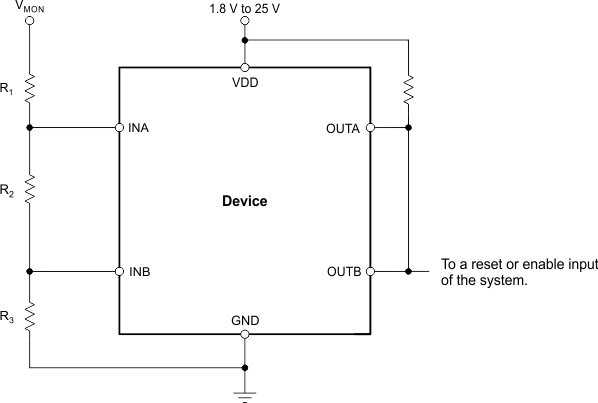
Figure 21 to Figure 24 show examples of the various input and output configurations.
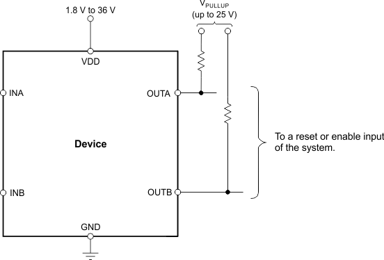
TPS3701 typ_app3_bvs240.gifFigure 21. Interfacing to Voltages Other than VDD
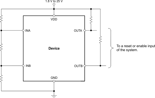
TPS3701 typ_app4_bvs240.gifFigure 22. Monitoring the Same Voltage as VDD
TPS3701 typ_app5_bvs240.gif

NOINDENT:

NOTE: The inputs can monitor a voltage higher than VDD (max) with the use of an external resistor divider network.
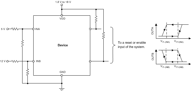
Figure 23. Monitoring a Voltage Other than VDD
TPS3701 ai_mon_ov_bvs240.gif

NOINDENT:

NOTE: In this case, OUTA is driven low when an undervoltage condition is detected at the 5-V rail and OUTB is driven low when an overvoltage condition is detected at the 12-V rail.
Figure 24. Monitoring Overvoltage for One Rail and Undervoltage for a Different Rail