SBVS250 April 2015 TPS3779 , TPS3780
PRODUCTION DATA.
- 1 Features
- 2 Applications
- 3 Description
- 4 Revision History
- 5 Device Comparison Table
- 6 Pin Configuration and Functions
- 7 Specifications
- 8 Detailed Description
- 9 Application and Implementation
- 10Power-Supply Recommendations
- 11Layout
- 12Device and Documentation Support
- 13Mechanical, Packaging, and Orderable Information
パッケージ・オプション
メカニカル・データ(パッケージ|ピン)
サーマルパッド・メカニカル・データ
- DRY|6
発注情報
6 Pin Configuration and Functions
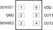
DRY Package
1.45-mm × 1-mm µSON
(Top View)

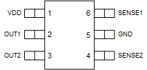
DBV Package
SOT23-6
(Top View)

Pin Functions
| PIN | I/O | DESCRIPTION | ||
|---|---|---|---|---|
| NAME | NO. | |||
| DRY | DBV | |||
| GND | 2 | 5 | — | Ground |
| OUT1 | 5 | 2 | O | OUT1 is the output for SENSE1. OUT1 is asserted (driven low) when the voltage at SENSE1 falls below VIT–. OUT1 is deasserted (goes high) after SENSE1 rises higher than VIT+. OUT1 is a push-pull output for the TPS3779 and an open-drain output for the TPS3780. The open-drain device (TPS3780) can be pulled up to 6.5 V independent of VDD; a pull-up resistor is required for this device. |
| OUT2 | 4 | 3 | O | OUT2 is the output for SENSE2. OUT2 is asserted (driven low) when the voltage at SENSE2 falls below VIT–. OUT2 is deasserted (goes high) after SENSE2 rises higher than VIT+. OUT2 is a push-pull output for the TPS3779 and an open-drain output for the TPS3780. The open-drain device (TPS3780) can be pulled up to 6.5 V independent of VDD; a pull-up resistor is required for this device. |
| SENSE1 | 1 | 6 | I | This pin is connected to the voltage to be monitored with the use of an external resistor divider. When the voltage at this pin drops below the threshold voltage (VIT–), OUT1 is asserted. |
| SENSE2 | 3 | 4 | I | This pin is connected to the voltage to be monitored with the use of an external resistor divider. When the voltage at this pin drops below the threshold voltage (VIT–), OUT2 is asserted. |
| VDD | 6 | 1 | I | Supply voltage input. Connect a 1.5-V to 6.5-V supply to VDD in order to power the device. Good analog design practice is to place a 0.1-µF ceramic capacitor close to this pin (required for VDD < 1.5 V). |