SBVS250 April 2015 TPS3779 , TPS3780
PRODUCTION DATA.
- 1 Features
- 2 Applications
- 3 Description
- 4 Revision History
- 5 Device Comparison Table
- 6 Pin Configuration and Functions
- 7 Specifications
- 8 Detailed Description
- 9 Application and Implementation
- 10Power-Supply Recommendations
- 11Layout
- 12Device and Documentation Support
- 13Mechanical, Packaging, and Orderable Information
パッケージ・オプション
メカニカル・データ(パッケージ|ピン)
サーマルパッド・メカニカル・データ
- DRY|6
発注情報
9 Application and Implementation
9.1 Application Information
The TPS3779 and TPS3780 are used as precision dual-voltage detectors. The monitored voltage, VDD voltage, and output pullup voltage (TPS3780 only) can be independent voltages or connected in any configuration.
9.1.1 Threshold Overdrive
Threshold overdrive is how much VDD exceeds the specified threshold, and is important to know because smaller overdrive results in slower OUTx response. Threshold overdrive is calculated as a percent of the threshold in question, as shown in Equation 1:
where
- VIT is either VIT– or VIT+, depending on whether calculating the overdrive for the negative-going threshold or the positive-going threshold, respectively.
Figure 16 illustrates the VDD minimum detectable pulse versus overdrive, and is used to visualize the relationship overdrive has on tPD(f) for negative-going events.
9.1.2 Sense Resistor Divider
The resistor divider values and target threshold voltage can be calculated by using Equation 2 and Equation 3 to determine VMON(UV) and VMON(PG), respectively.


where
- R1 and R2 are the resistor values for the resistor divider on the SENSEx pins,
- VMON(UV) is the target voltage at which an undervoltage condition is detected, and
- VMON(PG) is the target voltage at which the output goes high when VMONx rises.
Choose RTOTAL ( = R1 + R2) so that the current through the divider is approximately 100 times higher than the input current at the SENSEx pins. The resistors can have high values to minimize current consumption as a result of low input bias current without adding significant error to the resistive divider. For details on sizing input resistors, refer to application report SLVA450, Optimizing Resistor Dividers at a Comparator Input, available for download from www.ti.com.
9.2 Typical Applications
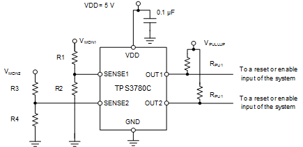
9.3 Monitoring Two Separate Rails
 Figure 22. Monitoring Two Separate Rails Schematic
9.3.1 Design Requirements
Table 2. Design Parameters
| PARAMETER | DESIGN REQUIREMENT | DESIGN RESULT |
|---|---|---|
| VDD | 5 V | 5 V |
| Hysteresis | 10% | 10% |
| Monitored voltage 1 | 3.3 V nominal, VMON(PG) = 2.9 V, VMON(UV) = 2.6 V | VMON(PG) = 2.908 V, VMON(UV) = 2.618 V |
| Monitored voltage 2 | 3 V nominal, VMON(PG) = 2.6 V, VMON(UV) = 2.4 V | VMON(PG) = 2.606 V, VMON(UV) = 2.371 V |
| Output logic voltage | 3.3-V CMOS | 3.3-V CMOS |
9.3.2 Detailed Design Procedure
- Select the TPS3780C. The C version is selected to satisfy the hysteresis requirement. The TPS3780 is selected for the output logic requirement. An open-drain output allows for the output to be pulled up to a voltage other than VDD.
- The resistor divider values are calculated by using Equation 2 and Equation 3. For SENSE1, R1 = 1.13 MΩ and R2 = 787 kΩ. For SENSE2, R3 (R1) = 681 kΩ and R4 (R2) = 576 kΩ.
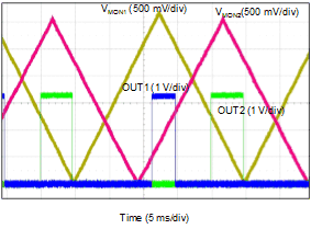
9.3.3 Application Curve
 Figure 23. Monitoring Two Separate Rails Curve
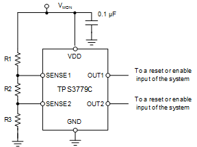
9.4 Early Warning Detection
 Figure 24. Early Warning Detection Schematic
9.4.1 Design Requirements
Table 3. Design Parameters
| PARAMETER | DESIGN REQUIREMENT | DESIGN RESULT |
|---|---|---|
| VDD | VMON | VMON |
| Hysteresis | 10% | 10% |
| Monitored voltage 1 | VMON(PG) = 3.3 V, VMON(UV) = 3 V | VMON(PG) = 3.330 V, VMON(UV) = 2.997 V |
| Monitored voltage 2 | VMON(PG) = 3.9 V, VMON(UV) = 3.5 V | VMON(PG) = 3.921 V, VMON(UV) = 3.529 V |
9.4.2 Detailed Design Procedure
- Select the TPS3779C. The C version is selected to satisfy the hysteresis requirement. The TPS3779 is selected to save on component count and board space.
- Use Equation 4 to calculate the total resistance for the resistor divider. Determine the minimum total resistance of the resistor network necessary to achieve the current consumption specification. For this example, the current flow through the resistor network is chosen to be 1.41 µA. Use the key transition point for VMON2. For this example, the low-to-high transition, VMON(PG), is considered more important.
- VMON(PG_2) is the target voltage at which OUT2 goes high when VMON2 rises, and
- I is the current flowing through the resistor network.
- After RTOTAL is determined, R3 can be calculated using Equation 5. Select the nearest 1% resistor value for R3. In this case, 845 kΩ is the closest value.
- Use Equation 6 to calculate R2. Select the nearest 1% resistor value for R2. In this case, 150 kΩ is the closest value. Use the key transition point for VMON1. For this example, the low-to-high transition, VMON(UV), is considered more important.
- VMON(UV_1) is the target voltage at which OUT1 goes low when VMON1 falls.
- Use Equation 7 to calculate R1. Select the nearest 1% resistor value for R1. In this case, 1.78 MΩ is a 1% resistor.

where


where

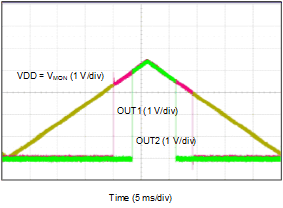
9.4.3 Application Curve
 Figure 25. Early Warning Detection Curve