JAJSMW7J December   2000  – August 2024 TPS3813

PRODUCTION DATA  

  1.   1
  2. 特長
  3. アプリケーション
  4. 概要
  5. Device Comparison Table
  6. Pin Configuration and Functions
  7. Specifications
    1. 6.1 Absolute Maximum Ratings
    2. 6.2 ESD Ratings
    3. 6.3 Recommended Operating Conditions
    4. 6.4 Thermal Information
    5. 6.5 Electrical Characteristics
    6. 6.6 Timing Requirements
    7. 6.7 Switching Characteristics
    8. 6.8 Dissipation Ratings
    9. 6.9 Typical Characteristics
  8. Detailed Description
    1. 7.1 Overview
    2. 7.2 Functional Block Diagram
    3. 7.3 Feature Description
      1. 7.3.1 Input Voltage (VDD)
        1. 7.3.1.1 VDD Hysteresis
        2. 7.3.1.2 VDD Glitch Immunity
      2. 7.3.2 User-Programmable Watchdog Timer (WDI)
      3. 7.3.3 RESET Output
    4. 7.4 Device Functional Modes
      1. 7.4.1 Normal Operation (VDD > VIT)
      2. 7.4.2 Above Power-On Reset But Less Than Threshold (VPOR < VDD < VIT)
      3. 7.4.3 Below Power-On Reset (VDD < VPOR)
    5. 7.5 Programming
      1. 7.5.1 Implementing Window-Watchdog Settings
      2. 7.5.2 Programmable Window-Watchdog by Using an External Capacitor
      3. 7.5.3 Lower Boundary Calculation
      4. 7.5.4 Watchdog Software Considerations
      5. 7.5.5 Power-Up Considerations
  9. Application and Implementation
    1. 8.1 Application Information
    2. 8.2 Typical Application
      1. 8.2.1 Design Requirements
      2. 8.2.2 Detailed Design Procedure
      3. 8.2.3 Application Curve
    3. 8.3 Power Supply Recommendations
    4. 8.4 Layout
      1. 8.4.1 Layout Guidelines
      2. 8.4.2 Layout Example
  10. Device and Documentation Support
    1. 9.1 Related Links
    2. 9.2 ドキュメントの更新通知を受け取る方法
    3. 9.3 サポート・リソース
    4. 9.4 Trademarks
    5. 9.5 静電気放電に関する注意事項
    6. 9.6 用語集
  11. 10Revision History
  12. 11Mechanical, Packaging, and Orderable Information

パッケージ・オプション

メカニカル・データ(パッケージ|ピン)
サーマルパッド・メカニカル・データ
発注情報

Typical Characteristics

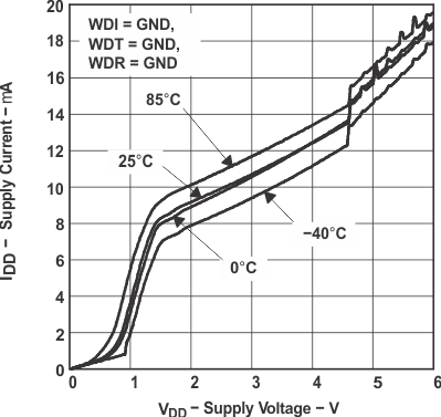
TPS3813 Supply Current vs Supply Voltage
Figure 6-2 Supply Current vs Supply Voltage
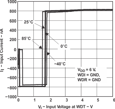
TPS3813 Input Current vs Input Voltage at WDT
Figure 6-4 Input Current vs Input Voltage at WDT
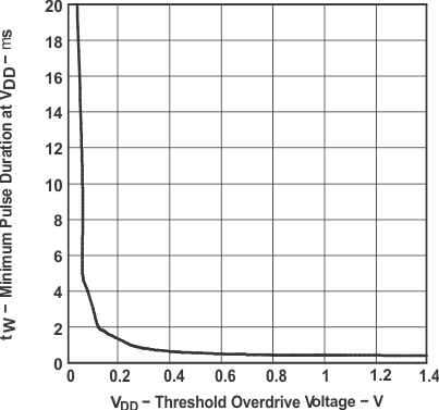
TPS3813 Minimum Pulse Duration at VDD vs VDD Threshold Overdrive Voltage
Figure 6-6 Minimum Pulse Duration at VDD vs VDD Threshold Overdrive Voltage
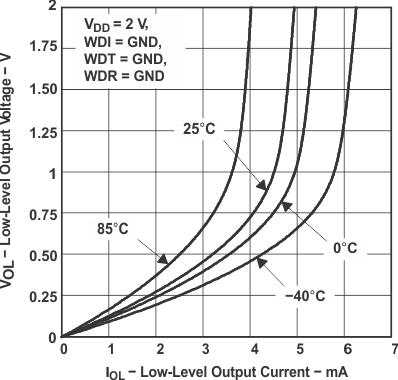
TPS3813 Low-Level Output Voltage vs Low-Level Output Current
Figure 6-3 Low-Level Output Voltage vs Low-Level Output Current
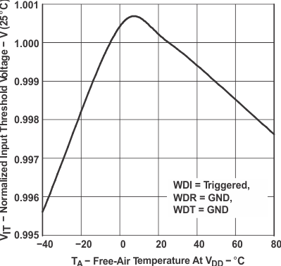
TPS3813 Normalized Input Threshold Voltage vs Free-Air Temperature at VDD
Figure 6-5 Normalized Input Threshold Voltage vs Free-Air Temperature at VDD