JAJSH97A April 2019 – September 2019 TPS3840-Q1
PRODUCTION DATA.
- 1 特長
- 2 アプリケーション
- 3 概要
- 4 改訂履歴
- 5 概要(続き)
- 6 Device Comparison Table
- 7 Pin Configuration and Functions
- 8 Specifications
- 9 Detailed Description
- 10Application and Implementation
- 11Power Supply Recommendations
- 12Layout
- 13デバイスおよびドキュメントのサポート
- 14メカニカル、パッケージ、および注文情報
8.7 Typical Characteristics
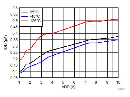
Typical characteristics show the typical performance of the TPS3840-Q1 device. Test conditions are TJ = 25°C, VDD = 3.3 V, Rpull-up = 100 kΩ, CLoad = 50 pF, unless otherwise noted. Figure 6. Supply Current vs Supply Voltage for TPS3840DL49-Q1
  Figure 8. Supply Current vs Supply Voltage for TPS3840PH49-Q1
  Figure 10. Negative-going Input Threshold Accuracy over Temperature for TPS3840PL-Q1
  Figure 12. Input Threshold VIT- Hysteresis Accuracy for TPS3840DL-Q1
  Figure 14. Input Threshold VIT- Hysteresis Accuracy for TPS3840PH-Q1
  Figure 16. Output Voltage vs Input Voltage for TPS3840PL49-Q1
  Figure 18. Low Level Output Voltage vs IRESET for TPS3840DL49-Q1
  Figure 20. Low Level Output Voltage vs IRESET for TPS3840PL49-Q1
  Figure 22. Low Level Output Voltage vs IRESET for TPS3840PH49-Q1
  Figure 24. High Level Output Voltage vs IRESET for TPS3840PL49-Q1
  Figure 26. High Level Output Voltage vs IRESET for TPS3840PH49-Q1
  Figure 28. Manual Reset Logic Low Voltage Threshold Over Temperature for TPS3840DL-Q1
  Figure 30. Manual Reset Logic Low Voltage Threshold Over Temperature for TPS3840PH-Q1
  Figure 32. Manual Reset Logic High Voltage Threshold Over Temperature for TPS3840PL-Q1
  Figure 34. Glitch Immunity on VIT- vs Overdrive (Data Taken with TPS3840PL28-Q1)
  Figure 36. Startup Delay Over Temperature
  Figure 38. Reset Time Delay vs Capacitor Value (Data Taken with TPS3840PL16-Q1)
  Figure 40. Reset Time Delay vs Large Capacitor Values (Data Taken with TPS3840PL16-Q1)
  Figure 42. Propagation Time Delay from MR Asserted to Reset Over Temperature
  Figure 7. Supply Current vs Supply Voltage for TPS3840PL49-Q1
  Figure 9. Negative-going Input Threshold Accuracy over Temperature for TPS3840DL-Q1
  Figure 11. Negative-going Input Threshold Accuracy over Temperature for TPS3840PH-Q1
  Figure 13. Input Threshold VIT- Hysteresis Accuracy for TPS3840PL-Q1
  Figure 15. Output Voltage vs Input Voltage for TPS3840DL49-Q1
  Figure 17. Output Voltage vs Input Voltage for TPS3840PH49-Q1
  Figure 19. Low Level Output Voltage vs VDD for TPS3840DL49-Q1
  Figure 21. Low Level Output Voltage vs VDD for TPS3840PL49-Q1
  Figure 23. Low Level Output Voltage vs VDD for TPS3840PH49-Q1
  Figure 25. High Level Output Voltage over Temperature for TPS3840PL49-Q1
  Figure 27. High Level Output Voltage Over Temperature for TPS3840PH49-Q1
  Figure 29. Manual Reset Logic Low Voltage Threshold Over Temperature for TPS3840PL-Q1
  Figure 31. Manual Reset Logic High Voltage Threshold Over Temperature for TPS3840DL-Q1
  Figure 33. Manual Reset Logic High Voltage Threshold Over Temperature for TPS3840PH-Q1
  Figure 35. CT Pin Internal Resistance Over Temperature
  Figure 37. Reset Time Delay with No Capacitor Over Temperature
  Figure 39. Reset Time Delay vs Small Capacitor Values (Data Taken with TPS3840PL16-Q1)
  Figure 41. Propagation Detect Time Delay for VDD Falling Below VIT- (High-to-Low) Over Temperature
  Figure 43. Propagation Time Delay from MR Release to Deasserted Reset Over Temperature