SBVS149B September 2010 – January 2016 TPS386000-Q1
PRODUCTION DATA.
- 1 Features
- 2 Applications
- 3 Description
- 4 Revision History
- 5 Pin Configuration and Functions
- 6 Specifications
- 7 Parametric Measurement information
- 8 Detailed Description
- 9 Application and Implementation
- 10Power Supply Recommendations
- 11Layout
- 12Device and Documentation Support
- 13Mechanical, Packaging, and Orderable Information
パッケージ・オプション
メカニカル・データ(パッケージ|ピン)
- RGP|20
サーマルパッド・メカニカル・データ
- RGP|20
発注情報
6 Specifications
6.1 Absolute Maximum Ratings
Over operating junction temperature range (unless otherwise noted) (1)| MIN | MAX | UNIT | |||
|---|---|---|---|---|---|
| Voltage | Input, VDD | –0.3 | 7 | V | |
| CT pin, VCT1, VCT2, VCT3, VCT4 | –0.3 | VDD + 0.3 | |||
| VRESET1, VRESET2, VRESET3, VRESET4, VMR, VSENSE1, VSENSE2, VSENSE3, VSENSE4L, VSENSE4H, VWDI, VWDO | –0.3 | 7 | |||
| Current | RESETn , RESETn, WDO, WDO, VREF pin current | 5 | mA | ||
| Power Dissipation | Continuous total | See Thermal Information Table. | |||
| Temperature | Operating virtual junction, TJ (2) | –40 | 150 | °C | |
| Operating ambient, TA | –40 | 125 | |||
| Storage, Tstg | –65 | 150 | |||
(1) Stresses beyond those listed under Absolute Maximum Ratings may cause permanent damage to the device. These are stress ratings only, which do not imply functional operation of the device at these or any other conditions beyond those indicated under Recommended Operating Conditions. Exposure to absolute-maximum-rated conditions for extended periods may affect device reliability.
(2) As a result of the low dissipated power in this device, it is assumed that TJ = TA.
6.2 ESD Ratings
| VALUE | UNIT | ||||
|---|---|---|---|---|---|
| V(ESD) | Electrostatic discharge | Human-body model (HBM), per AEC Q100-002(1) | ±2000 | V | |
| Charged-device model (CDM), per AEC Q100-011 | All pins | ±500 | |||
| Corner pins (1, 5, 6, 10, 11, 15, 16) | ±750 | ||||
(1) AEC Q100-002 indicates that HBM stressing shall be in accordance with the ANSI/ESDA/JEDEC JS-001 specification.
6.3 Recommended Operating Conditions
over operating free-air temperature range (unless otherwise noted)| MIN | NOM | MAX | UNIT | |||
|---|---|---|---|---|---|---|
| VDD | Supply voltage | 1.8 | 6.5 | V | ||
| Reset delay programming | CT1, CT2, CT3, CT4 | 0 | VDD | V | ||
| Manual reset input | MR | 0 | VDD | V | ||
| Watchdog timer trigger input WDI | 0 | VDD | V | |||
| TA | Operating free-air temperature | –40 | 125 | °C | ||
| TJ | Operating junction temperature | –40 | 150 | °C | ||
6.4 Thermal Information
| THERMAL METRIC(1) | TPS386000-Q1 | UNIT | |
|---|---|---|---|
| RGP (VQFN) | |||
| 20 PINS | |||
| RθJA | Junction-to-ambient thermal resistance | 50.8 | °C/W |
| RθJC(top) | Junction-to-case (top) thermal resistance | 1.5 | °C/W |
| RθJB | Junction-to-board thermal resistance | 21.0 | °C/W |
| ψJT | Junction-to-top characterization parameter | 42.8 | °C/W |
| ψJB | Junction-to-board characterization parameter | 8.8 | °C/W |
| RθJC(bot) | Junction-to-case (bottom) thermal resistance | 21.2 | °C/W |
(1) For more information about traditional and new thermal metrics, see the Semiconductor and IC Package Thermal Metrics application report, SPRA953.
6.5 Electrical Characteristics
Over the operating temperature range of TJ = –40°C to +125°C, 1.8 V < VDD < 6.5 V, RRESETn (n = 1, 2, 3, 4) = 100 kΩ to VDD, CRESETn (n = 1, 2, 3, 4L, 4H) = 50 pF to GND, RWDO = 100 kΩ to VDD, CWDO = 50 pF to GND, VMR = 100 kΩ to VDD, WDI = GND, and CTn (n = 1, 2, 3, 4) = open, unless otherwise noted. Typical values are at TJ = 25°C.| PARAMETER | TEST CONDITIONS | MIN | TYP | MAX | UNIT | |||
|---|---|---|---|---|---|---|---|---|
| VDD | Input supply range | 1.8 | 6.5 | V | ||||
| IDD | Supply current (current into VDD pin) | VDD = 3.3 V, RESETn or RESETn not asserted, WDI toggling(1), no output load, and VREF open | 11 | 19 | μA | |||
| VDD = 6.5 V, RESETn or RESETn not asserted, WDI toggling(1), no output load, and VREF open | 13 | 22 | ||||||
| Power-up reset voltage(2)(3) | VOL (max) = 0.2 V, IRESETn = 15 μA | 0.9 | V | |||||
| VIT– | Negative-going input threshold voltage | SENSE1, SENSE2, SENSE3, SENSE4L | 396 | 400 | 404 | mV | ||
| VIT+ | Positive-going input threshold voltage | SENSE4H | 396 | 400 | 404 | mV | ||
| VHYS– | Hysteresis (positive-going) on VIT– | SENSE1, SENSE2, SENSE3, SENSE4L | 3.5 | 10 | mV | |||
| VHYS+ | Hysteresis (negative-going) on VIT+ | SENSE4H | 3.5 | 10 | mV | |||
| ISENSE | Input current at SENSEm pin | VSENSEm = 0.42 V | –25 | ±1 | +25 | nA | ||
| ICT | CTn pin charging current | CT1 | CCT1 > 220 pF, VCT1 = 0.5 V(4) | 245 | 300 | 355 | nA | |
| CT2, CT3, CT4 | CCTn > 220 pF, VCTn = 0.5 V(4) | 235 | 300 | 365 | ||||
| VTH(CTn) | CTn pin threshold | CCTn > 220 pF | 1.18 | 1.238 | 1.299 | V | ||
| VIL | MR and WDI logic low input | 0 | 0.3 × VDD | V | ||||
| VIH | MR and WDI logic high input | 0.7 × VDD | V | |||||
| VOL | Low-level RESETn or RESETn output voltage | IOL = 1 mA | 0.4 | V | ||||
| SENSEn = 0V, 1.3 V < VDD < 1.8 V, IOL = 0.4 mA(2) |
0.3 | |||||||
| Low-level WDO output voltage | IOL = 1 mA | 0.4 | ||||||
| ILKG | RESETn, RESETn, WDO, and WDO leakage current | VRESETn = 6.5 V, RESETn, RESETn, WDO, and WDO are logic high | –300 | 300 | nA | |||
| VREF | Reference voltage output | 1 μA < IVREF < 0.2 mA (source only, no sink) | 1.18 | 1.20 | 1.22 | V | ||
| CIN | Input pin capacitance | CTn: 0 V to VDD, other pins: 0 V to 6.5 V | 5 | pF | ||||
(1) Toggling WDI for a period less than tWDT negatively affects IDD.
(2) These specifications are beyond the recommended VDD range, and only define RESETn or RESETn output performance during VDD ramp up.
(3) The lowest supply voltage (VDD) at which RESETn or RESETn becomes active; tRISE(VDD) ≥ 15 μs/V.
(4) CTn (where n = 1, 2, 3, or 4) are constant current charging sources working from a range of 0 V to VTH(CTn), and the device is tested at VCTn = 0.5 V. For ICT performance between 0V and VTH(CTn), see Figure 26.
6.6 Timing Requirements
Over operating temperature range of TJ = –40°C to 125°C, 1.8 V < VDD < 6.5 V, RRESETn (n = 1, 2, 3, 4) = 100 kΩ to VDD, CRESETn (n = 1, 2, 3, 4L, 4H) = 50 pF to GND, RWDO = 100 kΩ to VDD, CWDO = 50 pF to GND, VMR = 100 kΩ to VDD, WDI = GND, and CTn (n = 1, 2, 3, 4) = open, unless otherwise noted. Nominal values are at TJ = 25°C.| MIN | NOM | MAX | UNIT | |||
|---|---|---|---|---|---|---|
| tW | Input pulse width to SENSEm and MR pins | SENSEm: 1.05 VIT– → 0.95 VIT– or 0.95 VIT+ → 1.05 VIT+ |
4 | μs | ||
| MR: 0.7 VDD → 0.3 VDD | 1 | ns | ||||
6.7 Switching Characteristics
Over operating temperature range of TJ = –40°C to 125°C, 1.8 V < VDD < 6.5 V, RRESETn (n = 1, 2, 3, 4) = 100 kΩ to VDD, CRESETn (n = 1, 2, 3, 4L, 4H) = 50 pF to GND, RWDO = 100 kΩ to VDD, CWDO = 50 pF to GND, VMR = 100 kΩ to VDD, WDI = GND, and CTn (n = 1, 2, 3, 4) = open, unless otherwise noted. Typical values are at TJ = 25°C.| PARAMETER | TEST CONDITIONS | MIN | TYP | MAX | UNIT | |
|---|---|---|---|---|---|---|
| tD | RESETn or RESETn delay time | CTn = Open | 14 | 20 | 24 | ms |
| CTn = VDD | 225 | 300 | 375 | |||
| tWDT | Watchdog timer time-out period(1) | 450 | 600 | 750 | ms | |
(1) Start from RESET1 or RESET1 release or last WDI transition.
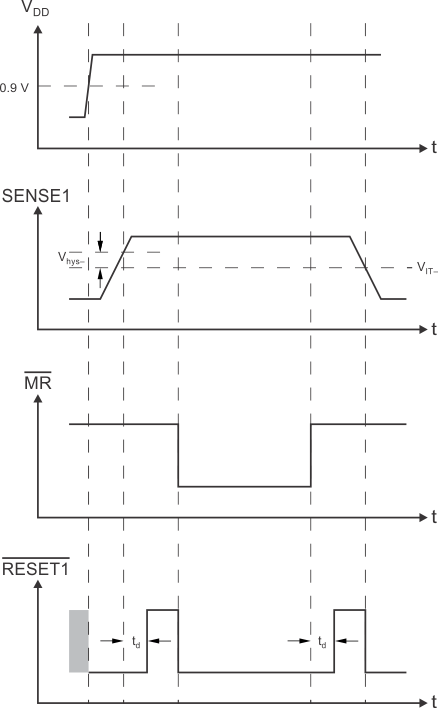
NOTE: The TPS386000-Q1 is shown here using RESETn.
Figure 1. SVS-1 Timing Diagram
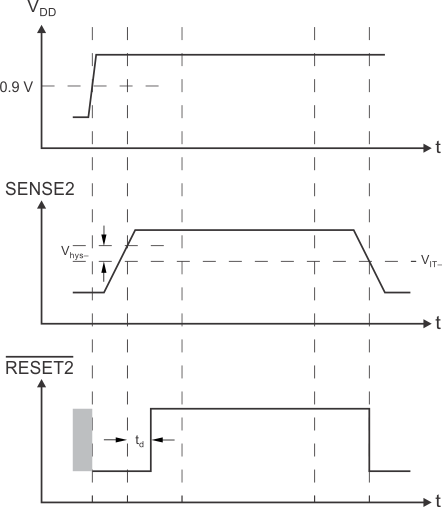
NOTE: The TPS386000-Q1 is shown here using RESETn.
Figure 2. SVS-2 Timing Diagram
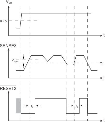
NOTE: The TPS386000-Q1 is shown here using RESETn.
Figure 3. SVS-3 Timing Diagram
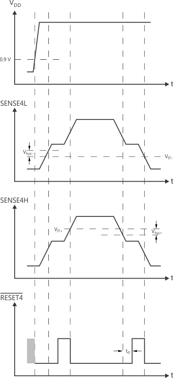
NOTE: The TPS386000-Q1 is shown here using RESETn.
Figure 4. SVS-4 Timing Diagram
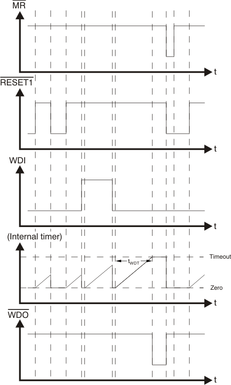
NOTE: The TPS386000-Q1 is shown here using RESETn and WDO.
Figure 5. WDT Timing Diagram
6.8 Typical Characteristics
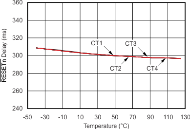
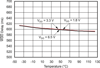
At TA = +25°C, and VDD = 3.3 V, unless otherwise noted.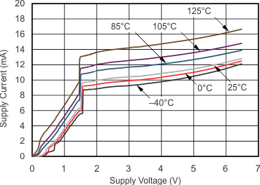
| UVLO released at approximately 1.5 V. |
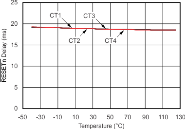
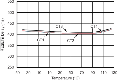
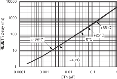
| These curves contain variance of capacitor values |
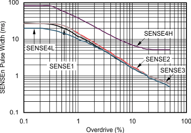
| See Figure 5 for the measurement technique. |
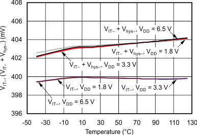
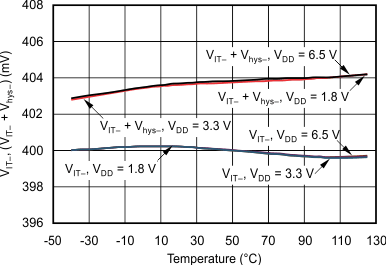
| 2 mV » 0.5% |
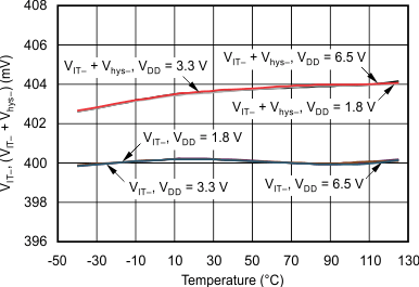
| 2 mV » 0.5% |
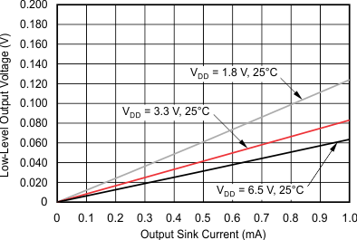
| All RESETn and WDO |
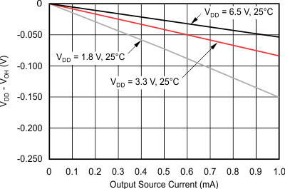
| All RESETn and WDO |
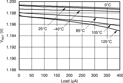
| Y-axis (1.188 V to 1.2 V) is 1% of 1.2 V |
(VDD = 1.8 V)
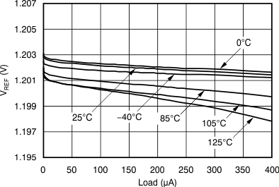
| Y-axis (1.195 V to 1.207 V) is 1% of 1.2 V |
(VDD = 6.5 V)
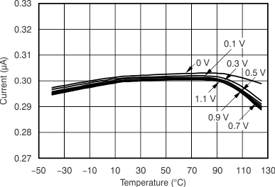
| Minimum and maximum values of the Y-axis are ±10% of 0.3 mA |
| 2 mV » 0.5% |
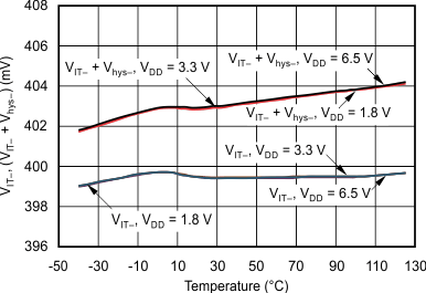
| 2 mV » 0.5% |
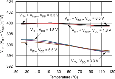
| 2 mV » 0.5% |
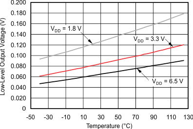
| All RESETn and WDO |
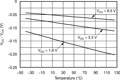
| All RESETn, RESETn, WDO, and WDO |
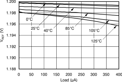
| Y-axis (1.188 V to 1.2 V) is 1% of 1.2 V |
(VDD = 3.3 V)
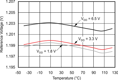
| Y-axis (1.195 V to 1.207 V) is 1% of 1.2 V |