JAJSHQ7A July   2019  – September 2019 TPS3870-Q1

PRODUCTION DATA.  

  1. 特長
  2. アプリケーション
  3. 概要
    1.     Device Images
      1.      過電圧検出機能を内蔵
      2.      過電圧精度の標準的な分散
  4. 改訂履歴
  5. 概要(続き)
  6. Device Comparison Table
  7. Pin Configuration and Functions
    1.     Pin Functions
  8. Specifications
    1. 8.1 Absolute Maximum Ratings
    2. 8.2 ESD ratings
    3. 8.3 Recommended Operating Conditions
    4. 8.4 Thermal Information
    5. 8.5 Electrical Characteristics
    6. 8.6 Timing Requirements
    7. 8.7 Typical Characteristics
  9. Detailed Description
    1. 9.1 Overview
    2. 9.2 Functional Block Diagram
    3. 9.3 Feature Description
      1. 9.3.1 VDD
      2. 9.3.2 SENSE
      3. 9.3.3 RESET
      4. 9.3.4 Capacitor Time (CT)
      5. 9.3.5 Manual Reset (MR)
    4. 9.4 Device Functional Modes
      1. 9.4.1 Normal Operation (VDD > VDD(MIN))
      2. 9.4.2 Undervoltage Lockout (VPOR < VDD < UVLO)
      3. 9.4.3 Power-On Reset (VDD < VPOR)
  10. 10Application and Implementation
    1. 10.1 Application Information
      1. 10.1.1 Voltage Threshold Accuracy
      2. 10.1.2 CT Reset Time Delay
        1. 10.1.2.1 Factory-Programmed Reset Delay Timing
        2. 10.1.2.2 Programmable Reset Delay-Timing
      3. 10.1.3 RESET Latch Mode
      4. 10.1.4 Adjustable Voltage Thresholds
      5. 10.1.5 Immunity to SENSE Pin Voltage Transients
        1. 10.1.5.1 Hysteresis
    2. 10.2 Typical Application
      1. 10.2.1 Design 1: RESET Latch Mode
        1. 10.2.1.1 Design Requirements
        2. 10.2.1.2 Detailed Design Procedure
        3. 10.2.1.3 Application Curves
  11. 11Power Supply Recommendations
    1. 11.1 Power Supply Guidelines
  12. 12Layout
    1. 12.1 Layout Guidelines
    2. 12.2 Layout Example
  13. 13デバイスおよびドキュメントのサポート
    1. 13.1 デバイスの項目表記
    2. 13.2 ドキュメントのサポート
      1. 13.2.1 評価基板
    3. 13.3 ドキュメントの更新通知を受け取る方法
    4. 13.4 サポート・リソース
    5. 13.5 商標
    6. 13.6 静電気放電に関する注意事項
    7. 13.7 Glossary
  14. 14メカニカル、パッケージ、および注文情報

パッケージ・オプション

メカニカル・データ(パッケージ|ピン)
サーマルパッド・メカニカル・データ
発注情報

Manual Reset (MR)

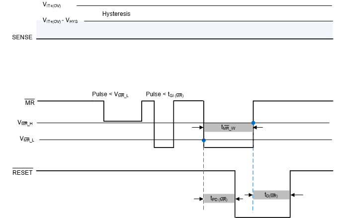
The manual reset (MR) input allows a processor or other logic circuits to initiate a reset. A logic low on MR causes RESET to assert. After MR returns to a logic high and the SENSE pin voltage is within a valid condition (VSENSE < VIT+(OV)) , RESET is deasserted after the reset delay time (tD). If MR is not controlled externally, then MR can either be connected to VDD or left floating because the MR pin is internally pulled up to VDD. Figure Figure 19 shows the relation between MR and RESET.
TPS3870-Q1 MR-Timing.gif
RESET pulls up to VDD with 10 kΩ.
To initiate and continue time reset counter both conditions must be met MR pin above VMR_H or floating and VSENSE below VIT+(OV) - VHYS
MR is ignored during output RESET low event
Figure 19. Manual Reset Timing Diagram