JAJSHQ7A July 2019 – September 2019 TPS3870-Q1
PRODUCTION DATA.
- 1 特長
- 2 アプリケーション
- 3 概要
- 4 改訂履歴
- 5 概要(続き)
- 6 Device Comparison Table
- 7 Pin Configuration and Functions
- 8 Specifications
- 9 Detailed Description
- 10Application and Implementation
- 11Power Supply Recommendations
- 12Layout
- 13デバイスおよびドキュメントのサポート
- 14メカニカル、パッケージ、および注文情報
10.1.4 Adjustable Voltage Thresholds
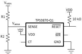
The TPS3870-Q1 0.7% maximum accuracy allows for adjustable voltage thresholds using external resistors without adding major inaccuracies to the device. In case that the desired monitored voltage is not available, external resistor dividers can be used to set the desired voltage thresholds. Figure 23 illustrates an example of how to adjust the voltage threshold with external resistor dividers. The resistors can be calculated depending on the desired voltage threshold and device part number. TI recommends using the 0.8V voltage threshold device such as the TPS3870J4080 because of the bypass mode of internal resistor ladder.
For example, consider a 2.0 V rail being monitored (VMON) using the TPS3870J4080 variant. Using Equation 4, R1 = 15 kΩ given that R2 = 10 kΩ, VMON = 2 V , and VSENSE = 0.8 V. This device is typically meant to monitor a 0.8 V rail with a +4% voltage threshold. This means that the device overvoltage threshold (VIT+(OV)) is 0.832 V. Using Equation 4, the monitored overvoltage threshold (VMON+) = 2.08 V when VSENSE = VIT+(OV). If a wider tolerance threshold is desired, use a device variant shown on Table 6 to determine what device part number matches your application.
There are inaccuracies that must be taken into consideration while adjusting voltage thresholds. Aside from the tolerance of the resistor divider, there is an internal resistance of the SENSE pin that may affect the accuracy of the resistor divider. Although expected to be very high impedance, users are recommended to calculate the values for design specifications. The internal sense resistance (RSENSE) can be calculated by the sense voltage (VSENSE) divided by the sense current (ISENSE) as shown in Equation 6. VSENSE can be calculated using Equation 4 depending on the resistor divider and monitored voltage. ISENSE can be calculated using Equation 5.
 Figure 23. Adjustable Voltage Threshold with External Resistor Dividers
 Although Equation 4 solves for VSENSE, inaccuracies for leakage need to be taken into consideration when understanding the overall threshold accuracy of the device. To calculate the threshold with this inaccuracy taken into account, use Equation 7
To calculate the worst case values through the resistor divider, ISENSE should be taken from the Electrical Characteristics table. While these equations provide a summary of what you need to correctly account for factors that go into determining your resistor divider with inaccuracy, you should use the Application Report Optimizing Resistor Dividers at a Comparator Input to further understand this and to design your implementation. This report explains how to optimize the resistor divider at the SENSE input for an adjustable voltage threshold version of the device. You should follow this Application Report using 0.8 V as the VREF value for the TPS3870-Q1.