JAJS194E January 2007 – June 2019 TPS40077
PRODUCTION DATA.
- 1 特長
- 2 アプリケーション
- 3 概要
- 4 改訂履歴
- 5 Pin Configuration and Functions
- 6 Specifications
-
7 Detailed Description
- 7.1 Overview
- 7.2 Functional Block Diagram
- 7.3
Feature Description
- 7.3.1 Minimum Pulse Duration
- 7.3.2 Slew Rate Limit On VDD
- 7.3.3 Setting The Switching Frequency (Programming The Clock Oscillator)
- 7.3.4 Loop Compensation
- 7.3.5 Shutdown and Sequencing
- 7.3.6 Boost and LVBP Bypass Capacitance
- 7.3.7 Internal Regulators
- 7.3.8 Power Dissipation
- 7.3.9 Boost Diode
- 7.3.10 Synchronous Rectifier Control
- 7.4 Programming
-
8 Application and Implementation
- 8.1 Application Information
- 8.2
Typical Applications
- 8.2.1
Buck Regulator 8-V to 16-V Input, 1.8-V Output at 10 A
- 8.2.1.1 Design Requirements
- 8.2.1.2
Detailed Design Procedure
- 8.2.1.2.1
Power Train Components
- 8.2.1.2.1.1 Output Inductor, LOUT
- 8.2.1.2.1.2 Output Capacitor, COUT, ELCO and MLCC
- 8.2.1.2.1.3 Input Capacitor, CIN ELCO and MLCC
- 8.2.1.2.1.4 Switching MOSFET, QSW
- 8.2.1.2.1.5 Rectifier MOSFET, QSR
- 8.2.1.2.1.6 Timing Resistor, RT
- 8.2.1.2.1.7 Feed-Forward and UVLO Resistor, RKFF
- 8.2.1.2.1.8 Soft-Start Capacitor, CSS
- 8.2.1.2.1.9 Short-Circuit Protection, RILIM and CILIM
- 8.2.1.2.1.10 Boost Voltage, CBOOST and DBOOST (Optional)
- 8.2.1.2.1.11 Closing the Feedback Loop, RZ1, RP1, RPZ2, RSET1, RSET2, CZ2, CP2, and CPZ1
- 8.2.1.2.1
Power Train Components
- 8.2.1.3 Application Curves
- 8.2.1
Buck Regulator 8-V to 16-V Input, 1.8-V Output at 10 A
- 8.3 Additional System Examples
- 9 Layout
- 10デバイスおよびドキュメントのサポート
- 11メカニカル、パッケージ、および注文情報
7.4.3 Programming Short-Circuit Protection
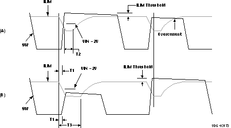
The TPS40077 uses a two-tier approach for short-circuit protection. The first tier is a pulse-by-pulse protection scheme. Short-circuit protection is implemented on the high-side MOSFET by sensing the voltage drop across the MOSFET when its gate is driven high. The MOSFET voltage is compared to the voltage dropped across a resistor (RILIM) connected from VVDD to the ILIM pin when driven by a constant-current sink. If the voltage drop across the MOSFET exceeds the voltage drop across the ILIM resistor, the switching pulse is immediately terminated. The MOSFET remains off until the next switching cycle is initiated. This is illustrated in Figure 26.
 Figure 26. Switching and Current-Limit Waveforms and Timing Relationship
 In addition, just prior to the high-side MOSFET turning on, the ILIM pin is pulled down to approximately half of VVDD. The ILIM pin is allowed to return to its nominal value after one of two events occurs. If the SW node rises to within approximately 2 V of VVDD, the device allows ILIM to go back to its nominal value. This is illustrated in Figure 26(A). T1 is the delay time from the internal PWM signal being asserted and the rise of SW. This includes a driver delay of 50 ns, typical. T2 is the reaction time of the sensing circuit that allows ILIM to start to return to its nominal value, typically 20 ns. The second event that can cause ILIM to return to its nominal value is for an internal timeout to expire. This is illustrated in Figure 26(B) as T3. Here SW never rises to VVDD – 2 V, for whatever reason, and the internal timer times out, releasing the ILIM pin.
Prior to ILIM starting back to its nominal value, overcurrent sensing is not enabled. In normal operation, this ensures that the SW node is at a higher voltage than ILIM when overcurrent sensing starts, avoiding false trips while allowing for a quicker blanking delay than would ordinarily be possible. Placing a capacitor across RILIM sets an exponential approach to the normal voltage at the ILIM pin. This exponential decay of the overcurrent threshold can be used to compensate for ringing on the SW node after its rising edge and to help compensate for slower-turnon FETs. Choosing the proper capacitance requires care. If the capacitance is too large, the voltage at ILIM does not approach the desired overcurrent level quickly enough, resulting in an apparent shift in overcurrent threshold as pulse duration changes. As a general rule, it is best to make the time constant of the R-C at the ILIM pin 0.2 times or less of the nominal pulse duration of the converter as shown in Equation 17.
Also, the comparator that uses ILIM and SW to determine if an overcurrent condition exists has a clamp on its SW input. This clamp makes the SW node never appear to fall more than 1.4 V (approximately, could be as much as 2 V at –40°C) below VVDD. When ILIM is more than 1.4 V below VVDD, the overcurrent circuit is effectively disabled.
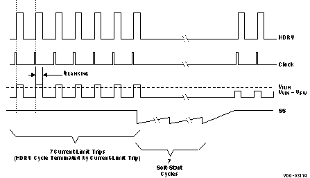
The second-tier protection incorporates a fault counter. The fault counter is incremented on each cycle with an overcurrent pulse and decremented on a clock cycle without an overcurrent pulse. When the counter reaches seven (7), a fault condition is declared by the controller. When this happens, the outputs are placed in a state defined in Table 2. Seven soft-start cycles are initiated (without activity on the HDRV and LDRV outputs) and the PWM is disabled during this period. The counter is decremented on each soft-start cycle. When the counter is decremented to zero, the PWM is re-enabled and the controller attempts to restart. If the fault has been removed, the output starts up normally. If the output is still present, the counter counts seven overcurrent pulses and re-enters the second-tier fault mode. Refer to Figure 27 for typical fault-protection waveforms.
In Equation 13, the minimum short-circuit limit setpoint (ISCP(min)) depends on tSTART, COUT, VOUT, ripple current in the inductor (IRIPPLE), and the load current at turnon (ILOAD).

The short-circuit limit programming resistor (RILIM) is calculated from Equation 14.

where
- IILIM is the current into the ILIM pin (110 μA, typical)
- VILIM(offset) is the offset voltage of the ILIM comparator (–50 mV, typical)
- ISCP is the short-circuit protection current
To find the range of the overcurrent values, use Equation 15 and Equation 16.


The TPS40077 provides short-circuit protection only. Therefore, it is recommended that the minimum short-circuit protection level be placed at least 20% above the maximum output current required from the converter. The maximum output of the converter should be the steady state maximum output plus any transient specification that may exist.
The ILIM capacitor maximum value can be found from Equation 17.

Note that this is a recommended maximum value. If a smaller value can be used, it should be. For most applications, consider using half the maximum value above.
 Figure 27. Typical Fault Protection Waveforms