SLVS753C February 2007 – November 2016 TPS40180
PRODUCTION DATA.
- 1 Features
- 2 Applications
- 3 Description
- 4 Revision History
- 5 Pin Configuration and Functions
- 6 Specifications
-
7 Detailed Description
- 7.1 Overview
- 7.2 Functional Block Diagram
- 7.3
Feature Description
- 7.3.1 Current Sensing and Overcurrent Detection
- 7.3.2 Hiccup Fault Recovery
- 7.3.3 Selecting Current Sense Network Components
- 7.3.4 PGOOD Functionality
- 7.3.5 Output Overvoltage and Undervoltage Protection
- 7.3.6 Overtemperature Protection
- 7.3.7 eTRIM™
- 7.3.8 Connections Between Controllers for Stacking
- 7.3.9 VSH Line in the Multiphase
- 7.4 Device Functional Modes
- 7.5 Programming
-
8 Application and Implementation
- 8.1 Application Information
- 8.2
Typical Applications
- 8.2.1
Single Output Synchronous Buck Converter
- 8.2.1.1 Design Requirements
- 8.2.1.2
Detailed Design Procedure
- 8.2.1.2.1 Inductor Selection
- 8.2.1.2.2 Output Capacitor Selection
- 8.2.1.2.3 Input Capacitor Selection
- 8.2.1.2.4 MOSFET Selection
- 8.2.1.2.5
Peripheral Component Design
- 8.2.1.2.5.1 Switching Frequency Setting (RT)
- 8.2.1.2.5.2 Output Voltage Setting (FB)
- 8.2.1.2.5.3 Current Sensing Network Design (CS+, CS-)
- 8.2.1.2.5.4 Overcurrent Protection (ILIM)
- 8.2.1.2.5.5 VREG (PVCC)
- 8.2.1.2.5.6 BP5
- 8.2.1.2.5.7 Phase Select (PSEL)
- 8.2.1.2.5.8 VSHARE (VSH)
- 8.2.1.2.5.9 Powergood (PGOOD)
- 8.2.1.2.5.10 Undervoltage Lockout (UVLO)
- 8.2.1.2.5.11 Clock Synchronization (CLKIO)
- 8.2.1.2.5.12 Bootstrap Capacitor
- 8.2.1.2.5.13 Soft Start (SS)
- 8.2.1.2.5.14 Remote Sense
- 8.2.1.2.5.15 Feedback Compensator Design
- 8.2.1.3 Application Curves
- 8.2.2 Simultaneous Tracking With TPS40180 Devices
- 8.2.3 2-Phase Single Output With TPS40180
- 8.2.1
Single Output Synchronous Buck Converter
- 9 Power Supply Recommendations
- 10Layout
- 11Device and Documentation Support
- 12Mechanical, Packaging, and Orderable Information
パッケージ・オプション
メカニカル・データ(パッケージ|ピン)
- RGE|24
サーマルパッド・メカニカル・データ
- RGE|24
発注情報
8 Application and Implementation
NOTE
Information in the following applications sections is not part of the TI component specification, and TI does not warrant its accuracy or completeness. TI’s customers are responsible for determining suitability of components for their purposes. Customers should validate and test their design implementation to confirm system functionality.
8.1 Application Information
The first design example describes the design process and component selection for a single-phase, synchronous buck, DC/DC converter using the TPS40180 device. The design process and component selection for a two-phase design are provided as well.
8.2 Typical Applications
8.2.1 Single Output Synchronous Buck Converter
Figure 32 illustrates the design process and component selection for a single output synchronous buck converter using TPS40180. The design goal parameters are given in Table 6. A list of symbol definitions is found in Device Nomenclature.
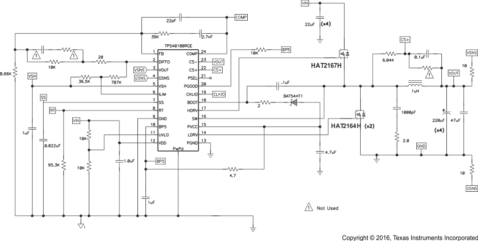 Figure 32. Single-Output Converter Schematic
8.2.1.1 Design Requirements
Table 6 lists the design parameters for the single output configuration from 12-V to 1.5-V DC-to-DC converter using a TPS40180.
Table 6. Design Goal Parameters
| PARAMETER | TEST CONDITIONS | MIN | TYP | MAX | UNIT | |
|---|---|---|---|---|---|---|
| VIN | Input voltage | 10.8 | 12 | 13.2 | V | |
| VOUT | Output voltage | 1.5 | V | |||
| VRIPPLE | Output ripple | IOUT = 20 A | 30 | mV | ||
| IOUT | Output current | 20 | A | |||
| fSW | Switching frequency | 280 | kHz | |||
8.2.1.2 Detailed Design Procedure
8.2.1.2.1 Inductor Selection
The inductor is determined by the desired ripple current. The required inductor is calculated by Equation 19.

Typically the peak-to-peak inductor current IRIPPLE is selected to be around 25% of the rated output current. In this design, IRIPPLE is targeted at 25% of IOUT. The calculated inductor is 0.95 µH and in practical a 1-µH inductor with 1.7-mΩ DCR from Vishay is selected. The real inductor ripple current is 4.7 A.
8.2.1.2.2 Output Capacitor Selection
The output capacitor is typically selected by the output load transient response requirement. Equation 20 estimates the minimum capacitor to reach the undervoltage requirement with load step-up. Equation 21 estimates the minimum capacitor for over voltage requirement with load step-down. When VIN(min) < 2 × VOUT, the minimum output capacitance can be calculated using Equation 20. Otherwise, Equation 21 is used.


In this design, VIN(min) is much larger than 2 × VOUT, so Equation 21 is used to determine the minimum capacitance. Based on a 8-A load transient with a maximum of 60-mV deviation, a minimum 356-µF output capacitor is required. Considering the capacitance variation and derating, four 220-µF, 4-V, SP capacitor are selected in the design to achieve sufficient margin. Each capacitor has an ESR of 5 mΩ.
Another criterion for capacitor selection is the output ripple voltage. The output ripple is determined mainly by the capacitance and the ESR. With an 880-µF output capacitance, the ripple voltage at the capacitor is calculated to be 1.5 mV. In the specification, the output ripple voltage should be less than 30 mV, so based on Equation 22, the required maximum ESR is 9.4 mΩ. The selected capacitors can meet this requirement.

8.2.1.2.3 Input Capacitor Selection
The input voltage ripple depends on input capacitance and ESR. The minimum capacitor and the maximum ESR can be estimated by Equation 23 and Equation 24.


For this design, assume VRIPPLE(Cin) is 100 mV and VRIPPLE(CinESR) is 50 mV, so the calculated minimum capacitance is 89 µF and the maximum ESR is 2.3 mΩ. Choosing four 22-µF, 16-V, 2-mΩ ESR ceramic capacitors meets this requirement.
Another important thing for the input capacitor is the RMS ripple current rating. The RMS current in the input capacitor is estimated with Equation 25.

where
- D is the duty cycle
The calculated RMS current is 6.6 A. Each selected ceramic capacitor has a RMS current rating of 4.3 A, so it is sufficient to reach this requirement.
8.2.1.2.4 MOSFET Selection
The MOSFET selection determines the converter efficiency. In this design, the duty cycle is very small so that the high-side MOSFET is dominated with switching losses and the low-side MOSFET is dominated with conduction loss. To optimize the efficiency, choose smaller gate charge for the high-side MOSFET and smaller RDS(on) for the low-side MOSFET. RENESAS HAT2167H and HAT2164H are selected as the high-side and low-side MOSFET respectively. The power losses in the high-side MOSFET is calculated with the following equations.
The RMS current in the high-side MOSFET is Equation 26.

The RDS(on)(sw) is 9.3 mΩ when the MOSFET gate voltage is 4.5 V. The conduction loss is Equation 27.

The switching loss is Equation 28.

The calculated total loss is the high-side MOSFET is Equation 29.

The RMS current in the low-side MOSFET is Equation 30.

The RDS(on)(sr) of each HAT2164 is 4.4 mΩ when the gate voltage is 4.5 V. Two HAT2164 FETs are used in this design.
The conduction loss in the low-side MOSFETs is Equation 31.

The total power loss in the body diode is Equation 32.

Therefore, the calculated total loss in the SR MOSFETs is Equation 33.

8.2.1.2.5 Peripheral Component Design
8.2.1.2.5.1 Switching Frequency Setting (RT)

In the design, a 95.3 kΩ resistor is selected. The actual switching frequency is 280 kHz.
8.2.1.2.5.2 Output Voltage Setting (FB)
Substitute the top resistor R1 with 10 kΩ in Equation 35, and then calculate the bottom bias resistor.

8.2.1.2.5.3 Current Sensing Network Design (CS+, CS–)
Choosing C1 a value for 0.1 µF, and calculating R with Equation 36.

8.2.1.2.5.4 Overcurrent Protection (ILIM)
ILIM pin is connected to VSH and VOUT pins with R1 and R2 respectively. Equation 8 and Equation 9 are used to calculate the overcurrent setting resistors. The DC over current rating is set at 28 A. The calculated values are 41 kΩ and 830 kΩ for R1 and R2 respectively. In the final design, R1 and R2 are chosen as 36.5 kΩ and
787 kΩ for temperature and other tolerances compensation.
8.2.1.2.5.5 VREG (PVCC)
A 4.7-µF capacitor is recommended to filter noise.
8.2.1.2.5.6 BP5
A 4.7-Ω resistor and 1-µF capacitor is placed between V REG and BP5 as a low-pass filter.
8.2.1.2.5.7 Phase Select (PSEL)
If the board is configured as a clock master for a multiphase application, an 8-phase CLKIO signal is generated if PSEL pin is open, and a 6-phase CLKIO signal is generated if PSEL is tied to ground with a 29.4-kΩ resistor. If the board is stacked as a slave for a multiphase application, a different resistor value is selected. The PSEL resistor selection is illustrated in the previous datasheet section.
8.2.1.2.5.8 VSHARE (VSH)
A 1-µF capacitor is tied from VSHARE to GND.
8.2.1.2.5.9 Powergood (PGOOD)
The PGOOD pin is tied to BP5 with a 10-kΩ resistor.
8.2.1.2.5.10 Undervoltage Lockout (UVLO)
UVLO is connected to the input voltage with a resistor divider. The two resistors have the same value of 10 kΩ. When the input voltage is higher than 2 V, the internal linear regulator is enabled.
8.2.1.2.5.11 Clock Synchronization (CLKIO)
CLKIO is floating as no clock synchronization required for single output configuration.
8.2.1.2.5.12 Bootstrap Capacitor
A bootstrap capacitor is connected between the BOOT and SW pin. The bootstrap capacitor depends on the total gate charge of the high-side MOSFET and the amount of droop allowed on the bootstrap capacitor (see Equation 37).

Qg is 11 nC and is 0.2 V in the calculation. For this application, a 0.1-µF capacitor is selected.
8.2.1.2.5.13 Soft Start (SS)
To get about 1-ms soft-start time, a 22-nF capacitor is tied to SS pin (see Equation 38).

ISS is the soft-start current which is 15-µA typically. VREF is the reference voltage, 0.7 V.
8.2.1.2.5.14 Remote Sense
VOUT and GSNS are connected to the remote sensing output connector. DIFFO is connected to the output voltage setting resistor divider. If the differential amplifier is not used, VOUT and GSNS are suggested to be grounded, and DIFFO is left open.
8.2.1.2.5.15 Feedback Compensator Design
Peak current mode control method is employed in the controller. A small signal model is developed from the COMP signal to the output (see Equation 39).

The time constant is defined by Equation 40.

Equation 40 is applied when the PWM pulse width is shorter than the current loop delay. The current loop delay is typically 100 ns.
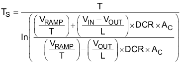
Equation 41 is applied when the PWM pulse width is longer than the current loop delay. The current loop delay is typically 100 ns. Equation 42 is used in this design because the PWM pulse width is much larger than the current loop delay. The low frequency pole is calculated by Equation 42.

The ESR zero is calculated by Equation 43.

In this design, at Type II compensator (Figure 33) is employed to compensate the loop.
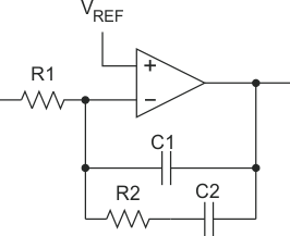 Figure 33. Type II Compensator
The compensator transfer function is Equation 44.

The loop gain function is Equation 45.

Assume the desired crossover frequency is 25 kHz, then set the compensator zero about 1/10 of the crossover frequency and the compensator pole equal to the ESR zero. The compensator gain is then calculated to achieve the desired bandwidth. In this design, the compensator gain, pole and zero are selected using Equation 46 through Equation 49.


From Equation 48, the compensator gain is solved as 4.5 × 10⁵.

Set R1 equal to 10 kΩ, and then calculate all the other components.
- R2 = 40 kΩ
- C1 = 22 pF
- C2 = 1.6 nF
In the real laboratory practice, the final components are selected as following to increase the phase margin and reduce PWM jitter.
- R1 = 10 kΩ
- R2 = 39 kΩ
- C1 = 22 pF
- C2 = 2.7 nF
8.2.1.3 Application Curves
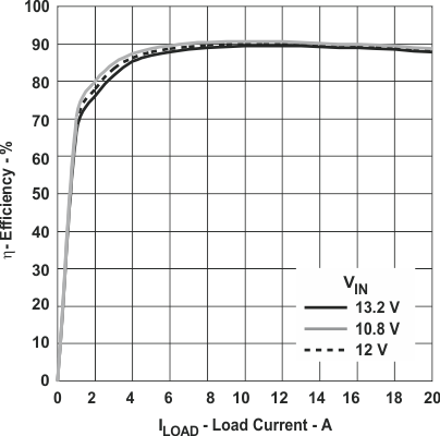 Figure 34. Efficiency Curve
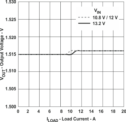 Figure 35. Output Load Regulation
8.2.2 Simultaneous Tracking With TPS40180 Devices
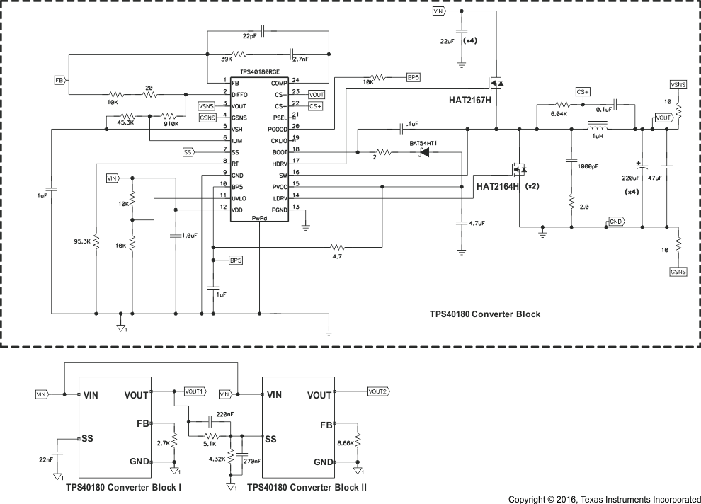 Figure 36. Simultaneous Tracking With TPS40180
8.2.2.1 Design Requirements
The TPS40180 can function in a tracking mode, where the output tracks some other voltage. In the simultaneous tracking design, the output voltages of two TPS40180 blocks needs to rise up and fall down with the same slew rate.
8.2.2.2 Detailed Design Procedure
In Figure 36, the SS pin of Block II is connected to the output voltage of Block I via voltage divider. A value between 1 kΩ and 10 kΩ is suggested for the bottom. Here a 4.32-kΩ resistor is selected for bottom resistor. From Equation 12, the top resistor is calculated as 5.1 kΩ.
From Equation 13, a 220-nF capacitor is selected in parallel with the top resistor, and a 270-nF capacitor is selected in parallel with bottom resistor.
8.2.2.3 Application Curves
8.2.3 2-Phase Single Output With TPS40180
In Figure 39, Block I and Block II are configured as master and slave respectively.
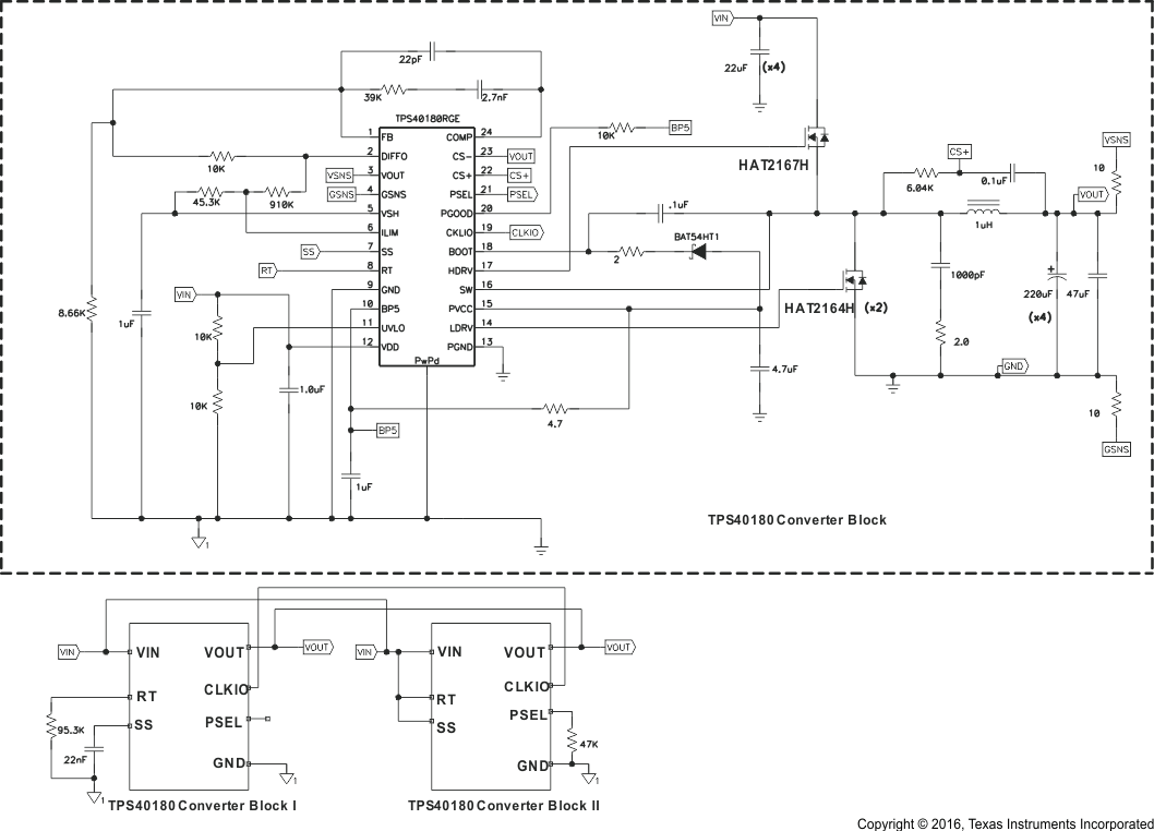 Figure 39. 2-Phase Single Output Schematic with TPS40180
VIN = 12 V, VOUT = 1.5 V, IOUT = 40 A
8.2.3.1 Design Requirements
Table 7 lists the design parameters for this example application.
Table 7. Design Goal Parameters
| PARAMETER | TEST CONDITIONS | MIN | TYP | MAX | UNIT | |
|---|---|---|---|---|---|---|
| VIN | Input voltage | 10.8 | 12 | 13.2 | V | |
| VOUT | Output voltage | 1.5 | V | |||
| VRIPPLE | Output ripple | IOUT = 40 A | 30 | mV | ||
| IOUT | Output current | 40 | A | |||
| fSW | Switching frequency | 280 | kHz | |||
8.2.3.2 Detailed Design Procedure
8.2.3.2.1 Inductor Selection
The inductor is determined by the desired inductor ripple current. Use Equation 19 to calculate the inductor value. In this design, IRIPPLE is targeted at 25% of phase current. The calculated inductor is 0.95 µH and in practical a 1-µH inductor with 1.7-mΩ DCR is selected. The real inductor ripple current is 4.7 A.
8.2.3.2.2 Output Capacitor Selection
The output capacitor is typically selected by the output load transient response requirement. Equation 21 in the single-phase design example is used. The inductor L in the equation is equal to the phase inductance divided by number of phases.
Based on a 40-A load transient with a maximum of 30 mV deviation, a minimum 711-µF output capacitor is required. Considering the capacitance variation and derating, eight 220-µF SP capacitors are selected in the design with sufficient margin. Each capacitor has an ESR of 5 mΩ.
Another criterion for capacitor selection is the output ripple voltage that is determined mainly by the capacitance and the ESR.
Due to the interleaving of channels, the total output ripple current is smaller than the ripple current from a single phase. The ripple cancellation factor is expressed in Equation 50. In this design, the ripple cancellation factor is 0.857.

where
- D is the duty cycle for a single phase
- NPH is the number of active phases, here it is equal to 2
- m = floor (NPH × D) is the maximum integer that does not exceed the (NPH × D), here m is 0
The output ripple current is then calculated in Equation 51. The maximum output ripple is with maximum input voltage. In this design, the maximum output ripple is calculated as 4.03 A.

With 1.76-mF output capacitance, the ripple voltage from the capacitance is 1 mV. In the specification, the output ripple voltage should be less than 30 mV, so based on Equation 22, the required maximum ESR is 7.2 mΩ. The selected capacitors must meet this requirement.
8.2.3.2.3 Input Capacitor Selection
The input voltage ripple depends on the input capacitance and ESR. The minimum capacitor and the maximum ESR can be estimated by Equation 23 and Equation 24 in the single phase design example. The phase current should be used in the calculation.
8.2.3.2.4 Peripheral Component Design
8.2.3.2.4.1 PSEL Pin
Use Table 3 and Table 4 to configure PSEL pin. In this design, the PSEL pin of master controller is open to set 8 phase CLKIO. The CLKIO pin sends out a pulse train for interleaving with 45° phase separation. The PSEL pin of slave controller is connected to GND through 47-kΩ resistor to set 180° phase angle.
8.2.3.2.4.2 CLKIO Pin
The CLKIO pins of master and slave controllers must be connected together. A 10-kΩ resistor is connected from the CLKIO line to GND to ensure that the CLKIO line falls to GND quickly when the master controller is shutdown or powers off.
8.2.3.2.4.3 RT Pin
In this design, the RT pin of master controller is connected to GND through 95.3-kΩ resistor to set switching frequency at 280 kHz per phase. The RT pin of slave controller is connected to VDD.
8.2.3.2.4.4 SS Pin
The SS pin of master controller is connected to GND through 22-nF capacitor to get about 1-ms soft-start time. The SS pin of slave parts to VDD pin is connected to VDD pin.
8.2.3.2.4.5 DIFFO Pin and FB Pin
The DIFFO pin and FB pin of master controller are connected to feedback and compensation network. The DIFFO pin and FB pin of slave controller are open.
8.2.3.2.4.6 COMP Pin
The COMP pins of master and slave controller must be connected together.
8.2.3.2.4.7 VSH Pin
An individual VSH bypass capacitor is required by master and slave controller. The VSH pins of master and slave controllers must be connected together.
8.2.3.2.4.8 Other Pins
Follow the design procedure of single-phase design for other peripheral components design.
8.2.3.3 Application Curves
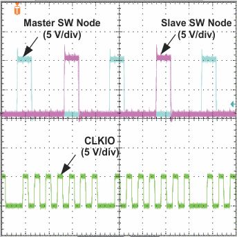 Figure 40. Switch Node and CLKIO Waveforms
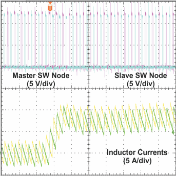 Figure 41. Current Balance at 0-A to 16-A Load
Step-Up, 2.5-A/µs Slew Rate