SLUS772G March 2008 – June 2020 TPS40210 , TPS40211
PRODUCTION DATA
- 1 Features
- 2 Applications
- 3 Description
- 4 Revision History
- 5 Pin Configuration and Functions
- 6 Specifications
-
7 Detailed Description
- 7.1 Overview
- 7.2 Functional Block Diagram
- 7.3
Feature Description
- 7.3.1 Soft Start
- 7.3.2 BP Regulator
- 7.3.3 Shutdown (DIS/ EN Pin)
- 7.3.4 Minimum On-Time and Off-Time Considerations
- 7.3.5 Setting the Oscillator Frequency
- 7.3.6 Synchronizing the Oscillator
- 7.3.7 Current Sense and Overcurrent
- 7.3.8 Current Sense and Subharmonic Instability
- 7.3.9 Current Sense Filtering
- 7.3.10 Control Loop Considerations
- 7.3.11 Gate Drive Circuit
- 7.3.12 TPS40211
- 7.4 Device Functional Modes
-
8 Application and Implementation
- 8.1 Application Information
- 8.2
Typical Applications
- 8.2.1
12-V to 24-V Nonsynchronous Boost Regulator
- 8.2.1.1 Design Requirements
- 8.2.1.2
Detailed Design Procedure
- 8.2.1.2.1 Custom Design with WEBENCH Tools
- 8.2.1.2.2 Duty Cycle Estimation
- 8.2.1.2.3 Inductor Selection
- 8.2.1.2.4 Rectifier Diode Selection
- 8.2.1.2.5 Output Capacitor Selection
- 8.2.1.2.6 Input Capacitor Selection
- 8.2.1.2.7 Current Sense and Current Limit
- 8.2.1.2.8 Current Sense Filter
- 8.2.1.2.9 Switching MOSFET Selection
- 8.2.1.2.10 Feedback Divider Resistors
- 8.2.1.2.11 Error Amplifier Compensation
- 8.2.1.2.12 RC Oscillator
- 8.2.1.2.13 Soft-Start Capacitor
- 8.2.1.2.14 Regulator Bypass
- 8.2.1.2.15 Bill of Materials
- 8.2.1.3 Application Curves
- 8.2.2 12-V Input, 700-mA LED Driver, Up to 35-V LED String
- 8.2.1
12-V to 24-V Nonsynchronous Boost Regulator
- 9 Power Supply Recommendations
- 10Layout
- 11Device and Documentation Support
- 12Mechanical, Packaging, and Orderable Information
デバイスごとのパッケージ図は、PDF版データシートをご参照ください。
メカニカル・データ(パッケージ|ピン)
- DRC|10
- DGQ|10
サーマルパッド・メカニカル・データ
7.3.1 Soft Start
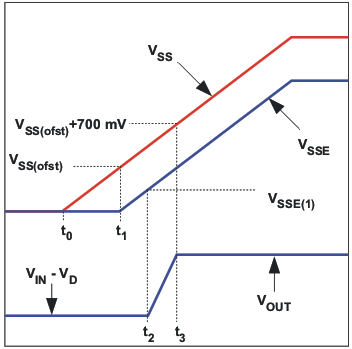
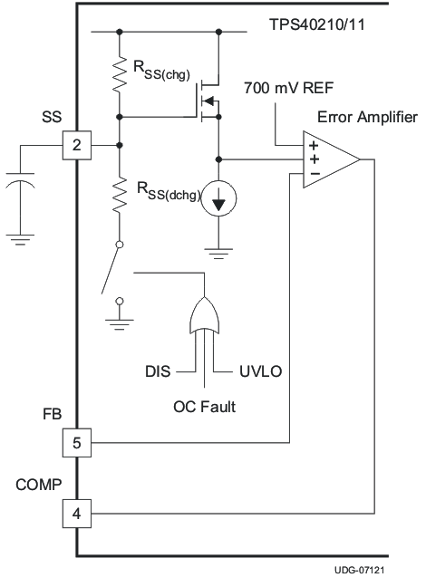
The soft-start feature of the TPS40210 and TPS40211 is a closed-loop soft start, meaning that the output voltage follows a linear ramp that is proportional to the ramp generated at the SS pin. This ramp is generated by an internal resistor connected from the BP pin to the SS pin and an external capacitor connected from the SS pin to GND. The SS pin voltage (VSS) is level shifted down by approximately VSS(ofst) (approximately 700 mV) and sent to one of the “+” (the “+” input with the lowest voltage dominates) inputs of the error amplifier. When this level shifted voltage (VSSE) starts to rise at time t1 (see Figure 7-1), the output voltage the controller expects, rises as well. Since VSSE starts at near 0 V, the controller attempts to regulate the output voltage from a starting point of zero volts. It cannot do this due to the converter architecture. The output voltage starts from the input voltage less the drop across the diode (VIN - VD) and rises from there. The point at which the output voltage starts to rise (t2) is the point where the VSSE ramp passes the point where it is commanding more output voltage than (VIN - VD). This voltage level is labeled VSSE(1). The time required for the output voltage to ramp from a theoretical zero to the final regulated value (from t1 to t3) is determined by the time it takes for the capacitor connected to the SS pin (CSS) to rise through a 700-mV range, beginning at VSS(ofst) above GND.
 Figure 7-1 SS Pin Voltage and Output Voltage
 Figure 7-2 SS Pin Functional Circuit
The required capacitance for a given soft-start time t3 – t1 in Figure 7-1 is calculated in Equation 1.

where
- tSS is the soft-start time, in seconds
- RSS(chg) is the SS charging resistance in Ω, typically 500 kΩ
- CSS is the value of the capacitor on the SS pin, in F
- VBP is the value of the voltage on the BP pin, in V
- VSS(ofst) is the approximate level shift from the SS pin to the error amplifier (~700 mV)
- VFB is the error amplifier reference voltage, 700 mV typical
Note that tSS is the time it takes for the output voltage to rise from 0 V to the final output voltage. Also note the tolerance on RSS(chg) given in the Section 6.5. This contributes to some variability in the output voltage rise time and margin must be applied to account for it in design.
Also take note of VBP. Its value varies depending on input conditions. For example, a converter operating from a slowly rising input initializes VBP at a fairly low value and increases during the entire startup sequence. If the controller has a voltage above 8 V at the input and the DIS pin is used to stop and then restart the converter, VBP is approximately 8 V for the entire start-up sequence. The higher the voltage on BP, the shorter the start-up time is and conversely, the lower the voltage on BP, the longer the start-up time is.
The soft-start time (tSS) must be chosen long enough so that the converter can start up without going into an overcurrent state. Since the over current state is triggered by sensing the peak voltage on the ISNS pin, that voltage must be kept below the overcurrent threshold voltage VISNS(oc). The voltage on the ISNS pin is a function of the load current of the converter, the rate of rise of the output voltage and the output capacitance, and the current sensing resistor. The total output current that must be supported by the converter is the sum of the charging current required by the output capacitor and any external load that must be supplied during start-up. This current must be less than the IOUT(oc) value used in Equation 15 or Equation 16 (depending on the operating mode of the converter) to determine the current sense resistor value. In these equations, the actual input voltage at the time that the controller reaches the final output voltage is the important input voltage to use in the calculations. If the input voltage is slowly rising and is at less than the nominal input voltage when the start-up time ends, the output current limit is less than IOUT(oc) at the nominal input voltage. The output capacitor charging current must be reduced (decrease COUT or increase the tSS) or IOUT(oc) must be increased and a new value for RISNS calculated.


where
- IC(chg) is the output capacitor charging current in A
- COUT is the total output capacitance in F
- VOUT is the output voltage in V
- tSS is the soft-start time from Equation 1
- IOUT(oc) is the desired over current trip point in A
- IEXT is any external load current in A
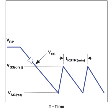
The capacitor on the SS pin (CSS) also plays a role in overcurrent functionality. It is used as the timer between restart attempts. The SS pin is connected to GND through a resistor, RSS(dchg), whenever the controller senses an overcurrent condition. Switching stops and nothing else happens until the SS pin discharges to the soft-start reset threshold, VSS(rst). At this point, the SS pin capacitor is allowed to charge again through the charging resistor RSS(chg), and the controller restarts from that point. The shortest time between restart attempts occurs when the SS pin discharges from VSS(ofst) (approximately 700 mV) to VSS(rst) (150 mV) and then back to VSS(ofst) and switching resumes. In actuality, this is a conservative estimate since switching does not resume until the VSSE ramp rises to a point where it is commanding more output voltage than exists at the output of the controller. This occurs at some SS pin voltage greater than VSS(ofst) and depends on the voltage that remains on the output overvoltage the converter while switching has been halted. The fastest restart time can be calculated by using Equation 4, Equation 5, and Equation 6.


 Figure 7-3 Soft Start during Overcurrent