SLVSBP4D December 2012 – September 2014 TPS43060 , TPS43061
PRODUCTION DATA.
- 1 Features
- 2 Applications
- 3 Description
- 4 Simplified Schematic
- 5 Revision History
- 6 Pin Configuration and Functions
- 7 Specifications
-
8 Detailed Description
- 8.1 Overview
- 8.2 Functional Block Diagram
- 8.3
Feature Description
- 8.3.1 Switching Frequency
- 8.3.2 Low-Dropout Regulator
- 8.3.3 Input Undervoltage (UV)
- 8.3.4 Enable and Adjustable UVLO
- 8.3.5 Voltage Reference and Setting Output Voltage
- 8.3.6 Minimum On-Time and Pulse Skipping
- 8.3.7 Zero-Cross Detection and Duty Cycle
- 8.3.8 Minimum Off-Time and Maximum Duty Cycle
- 8.3.9 Soft-Start
- 8.3.10 Power Good
- 8.3.11 Overvoltage Protection (OVP)
- 8.3.12 OVP and Current Sense Resistor Selection
- 8.3.13 Gate Drivers
- 8.3.14 Thermal Shutdown
- 8.4 Device Functional Modes
-
9 Application and Implementation
- 9.1 Application Information
- 9.2
Typical Applications
- 9.2.1
Synchronous Boost Converter Typical Application Using TPS43061
- 9.2.1.1 Design Requirements
- 9.2.1.2
Detailed Design Procedure
- 9.2.1.2.1 Selecting the Switching Frequency
- 9.2.1.2.2 Inductor Selection
- 9.2.1.2.3 Selecting the Current Sense Resistor
- 9.2.1.2.4 Output Capacitor Selection
- 9.2.1.2.5 MOSFET Selection - NexFET Power Block
- 9.2.1.2.6 Bootstrap Capacitor Selection
- 9.2.1.2.7 VCC Capacitor
- 9.2.1.2.8 Input Capacitor
- 9.2.1.2.9 Output Voltage and Feedback Resistors Selection
- 9.2.1.2.10 Setting the Soft-Start Time
- 9.2.1.2.11 UVLO Set Point
- 9.2.1.2.12 Power Good Resistor Selection
- 9.2.1.2.13 Control Loop Compensation
- 9.2.1.2.14 DCM, Pulse-Skip Mode, and No-Load Input Current
- 9.2.1.3 Application Curves
- 9.2.2 High-Efficiency 40-V Synchronous Boost Converter Typical Application Using TPS43060
- 9.2.1
Synchronous Boost Converter Typical Application Using TPS43061
- 10Power Supply Recommendations
- 11Layout
- 12Device and Documentation Support
- 13Mechanical, Packaging, and Orderable Information
パッケージ・オプション
メカニカル・データ(パッケージ|ピン)
- RTE|16
サーマルパッド・メカニカル・データ
- RTE|16
発注情報
11 Layout
11.1 Layout Guidelines
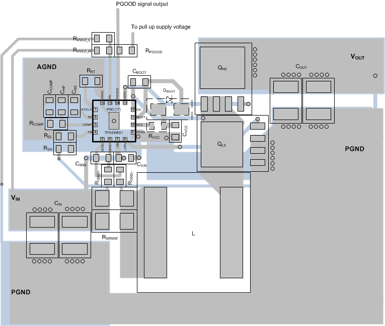
Layout is a critical portion of a good power converter design. Several signal paths that conduct fast changing currents or voltages can interact with stray inductance or parasitic capacitance to generate noise or degrade performance. Guidelines are as follows, and the EVM layouts can be used as a reference.
- The high-speed switching current path includes the high-side FET, low-side FET, and output capacitors. This is a critical loop to minimize in order to reduce noise and achieve best performance.
- Components connected to noise-sensitive circuitry should be located as close to the TPS4306x as possible, and be connected the AGND pin. This includes components connected to FB, COMP, SS, and RT/CLK pins.
- The PowerPAD should be connected to the quiet analog ground for the AGND pin to limit internal noise. For thermal performance, multiple vias directly under the device should be used to connect to any internal ground planes.
- Components in the power conversion path should be connected to the PGND. This includes the bulk input capacitors, output capacitors, low-side FET, and EN UVLO resistors.
- A single connection must connect the quiet AGND to the noisy PGND near the PGND pin.
- The low-ESR ceramic bypass capacitor for the VIN pin should be connected to the quiet AGND as close as possible to the TPS4306x.
- The distance between the inductor, low-side FET, and high-side FET should be minimized to reduce noise. This connection is the high-speed switching voltage node.
- The high-side and low-side FETs should be placed close to the device to limit the trace length required for the HDRV and LDRV gate drive signals.
- The bypass capacitor between the ISNS+ and ISNS– pins should be placed next to the TPS4306x. Minimize the distance between the device and the sense resistors.
11.2 Layout Example

NOTE
DBOOT and RVCC are only required if using the TPS43060.
11.3 Thermal Considerations
The TPS4306x junction temperature should not exceed 150°C under normal operating conditions. This restriction limits the power dissipation of the device. Power dissipation of the controller includes gate drive power loss and bias power loss of the internal VCC regulator. The TPS4306x is packaged in a thermally-enhanced WQFN package, which includes a PowerPAD that improves the thermal capabilities. The thermal resistance of the WQFN package depends on the PCB layout and the PowerPAD connection. As mentioned in the layout considerations, the PowerPAD must be soldered to the analog ground on the PCB with thermal vias underneath the PowerPAD to achieve good thermal performance.
For best thermal performance, PCB copper area should be sized to improve thermal capabilities of the components in the power path dissipating the most power. This includes the sense resistors, inductor, low-side FET, and high-side FET. Follow the manufacturer guidelines for the selected external FETs.