JAJS455B December 2009 – July 2017 TPS43331-Q1
PRODUCTION DATA.
- 1 特長
- 2 アプリケーション
- 3 概要
- 4 改訂履歴
- 5 Pin Configuration and Functions
-
6 Specifications
- 6.1 Absolute Maximum Ratings
- 6.2 ESD Ratings
- 6.3 Recommended Operating Conditions
- 6.4 Thermal Information
- 6.5 DC Electrical Characteristics
- 6.6 I2C Interface Electrical Characteristics
- 6.7 Switching Regulators Electrical Characteristics
- 6.8 Standby Regulator (VSTBY) Electrical Characteristics
- 6.9 Linear Regulator (VLR) Electrical Characteristics
- 6.10 High-Side Driver (HSD) Electrical Characteristics
- 6.11 AC Switching Characteristics
- 6.12 I2C Interface Switching Characteristics
- 6.13 Switching Regulators Switching Characteristics
- 6.14 Linear Regulator Switching Characteristics
- 6.15 High-Side Driver (HSD) Switching Characteristics
- 6.16 Timing and Switching Diagrams
- 6.17 Typical Characteristics
-
7 Detailed Description
- 7.1 Overview
- 7.2 Functional Block Diagram
- 7.3
Feature Description
- 7.3.1 Unregulated Battery Input Voltage (VBAT)
- 7.3.2 Protected Unregulated Battery Input Voltage (VBATP)
- 7.3.3 Low-Voltage Warning Input (LVWIN)
- 7.3.4 Voltage Warning Output (VBATW)
- 7.3.5 Low-Voltage Reset (RST)
- 7.3.6 Power-Good Delay Timer Input (PGDLY)
- 7.3.7 Active Mode Enable Input (EN)
- 7.3.8 Slew Rate Control Capacitor Input (CSLEW)
- 7.3.9 Charge Pump Capacitor Input (VCP)
- 7.3.10 Power Ground (PGND)
- 7.3.11 Analog Ground Reference (AGND)
- 7.3.12 Inter-IC Communications Interface (I2CID)
- 7.3.13 Clock Input (SCL)
- 7.3.14 Data Line (SDA)
- 7.3.15 Interface Chip Identifier (I2CID)
- 7.3.16 Switch Mode Regulators
- 7.3.17 Upper FET Gate Drive Outputs (VGT1 and VGT2)
- 7.3.18 Lower FET Gate Driver Outputs (VGB1 and VGB2)
- 7.3.19 Bootstrap Capacitor Input (CBS1 and CBS2)
- 7.3.20 Phase Reference for High-Side Bootstrap Supply (PH1 and PH2)
- 7.3.21 Current Sense High-Side (ISHI1 and ISHI2)
- 7.3.22 Current Sense Low-Side (ISLO1 and ISLO2)
- 7.3.23 Regulated Output Sense Voltage Feedback (VFB1 and VFB2)
- 7.3.24 Feedback Compensation Input (VCMP1 and VCMP2)
- 7.3.25 Synchronization Input (SYNCH)
- 7.3.26 Standby Linear Regulator Input (VINSB)
- 7.3.27 Standby Regulator Output (VSTBY)
- 7.3.28 Standby Regulator Sense Voltage (VSTBYS)
- 7.3.29 Switched Linear Regulator Input (VINLR)
- 7.3.30 Switched Linear Regulator Output (VLR)
- 7.3.31 Switched Linear Regulator Sense Voltage (VLRS)
- 7.3.32 High-Side Driver Output (HSD)
- 7.4 Device Functional Modes
- 7.5 Programming
- 7.6 Register Map
-
8 Application and Implementation
- 8.1 Application Information
- 8.2 Typical Application
- 8.3 System Example
- 9 Power Supply Recommendations
- 10Layout
- 11デバイスおよびドキュメントのサポート
- 12メカニカル、パッケージ、および注文情報
パッケージ・オプション
メカニカル・データ(パッケージ|ピン)
- DAP|38
サーマルパッド・メカニカル・データ
- DAP|38
発注情報
8 Application and Implementation
NOTE
Information in the following applications sections is not part of the TI component specification, and TI does not warrant its accuracy or completeness. TI’s customers are responsible for determining suitability of components for their purposes. Customers should validate and test their design implementation to confirm system functionality.
8.1 Application Information
The TPS43331-Q1 is a combination of two switched-mode, synchronous step-down controllers and two linearly-regulated power supplies. These devices are configured to drive external NMOS power switches and control the energy in the inductor by limiting the current using a resistor current sense feedback. The output voltage is regulated using an external resistor feedback network. The regulated output voltage can be programmed to a specified range using different feedback thresholds at the VFB(x) terminal. To minimize ripple current on the input line, the two buck regulators are switched 180º out of phase.
The protected high-side output is controlled by a discrete input to switch auxiliary input power to other devices in the system. The standby regulator VSTBY is enabled when the input power from the protected terminal of the battery supply is available to the device. The standby regulator consumes less than 75 μA, with less than 100 μA of load current on the regulated output terminal (VSTBY).
8.2 Typical Application
The calculations from the Buck Regulators section result in the schematic shown in Figure 20.
The design requirements for the switching regulator design in Figure 20 are listed in Table 3.
Assume Type III Compensation network for each buck regulator.
 Figure 20. Design Circuit Schematic
8.2.1 Design Requirements
For this design example, use the parameters listed in Table 3.
Table 3. Design Requirements
8.2.2 Detailed Design Procedure
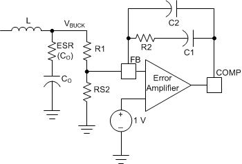
8.2.2.1 Type II Compensation
The LC output filter gives a Double Pole which has a –180° phase shift.

The ESR of the output capacitor, CO, gives a zero that has a 90° phase shift.

The values of R1 and RS2 are chosen based on the desired VBUCK.

where
- Vref = 1 V
Use the following equations to select the resistor vales:
Select RS2 = 10 kΩ


where
- Vramp = 1.8 V, VBAT = typical input operating voltage
- fc = fSW × 0.1 (the cutoff frequency, when the gain is 1 is called the unity gain frequency)
The fc is typically 1/5 to 1/10 of the switching frequency.
Use Equation 8 to calculate the PWM modulator gain (K).

Use Equation 9 to calculate the amplifier gain (Av).


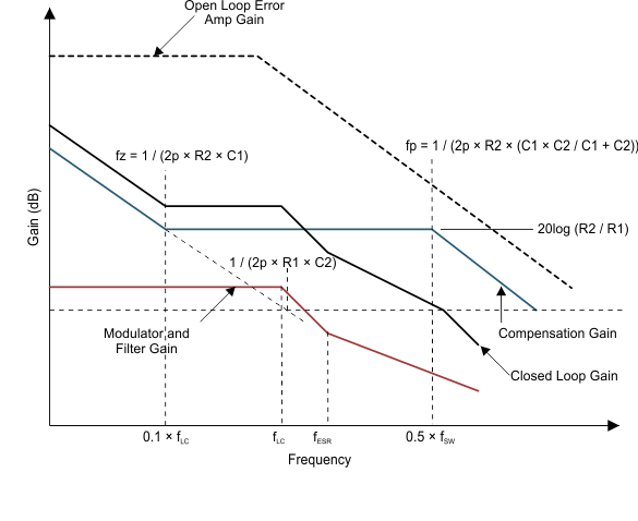 Figure 22. Type II Bode Plots
8.2.2.2 Type III Compensation
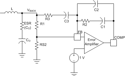 Figure 23. Type III Compensation
fc = fSW × 0.1 (the cutoff frequency when the gain is 1 is called the unity gain frequency).
The fc is typically 1/5 to 1/10 of the switching frequency double pole frequency response due to the LC output filter.
The LC output filter gives a Double Pole which has a –180° phase shift.

The ESR of the output capacitor, CO, gives a zero that has a 90° phase shift.


where
- Vref = 1 V
Use Equation 17 to calculate the PWM modulator gain (K).

where
- Vramp = 1.8 V
- VBAT = typical input operating voltage
Use Equation 18 to calculate the amplifier gain (Av).


Use the following guidelines for compensation components:
Make the two zeroes close to the double pole (LC); for example, fZ1 ≈ fZ2 ≈ 1 / 2π × (LCO)1/2.
- Make the first zero below the filter double pole (approximately 50% to 75% of fLC).
- Make the second zero at filter double pole (fLC).
Make the two poles above the cross-over frequency fc.
- Make the first pole at the ESR frequency (fESR).
- Make the second pole at 0.5 the switching frequency (0.5 × fSW).
Use the following equations to select the resistor values:
Select RS2 = 10 kΩ


Calculate C1 based on placing a zero at 50% to 75% of the output filter double pole frequency.

Calculate C2 by placing the first pole at the ESR zero frequency.

Set the second pole at 0.5 the switching frequency and also set the second zero at the output filter double pole frequency.


 Figure 24. Type III Bode Plots
8.2.2.3 Component Calculations
8.2.2.3.1 Buck-Controllers (VBUCK1, VBUCK2)
Use Equation 30 to calculate and select the desired inductor ripple current (ΔIL).
where
- IO(max) = Maximum output current
The typical inductor ripple current is between 20% to 40% of the maximum output current.
Use Equation 31 to calculate the value of the inductor (L).

where
- fSW is the switching frequency of the regulator
- Iripple = Allowable ripple current in the inductor, 20% to 40% of maximum IO(max)
Use Equation 32 to calculate the value of the the rms and peak current flowing in the inductor is.

Use Equation 33 to calculate the inductor peak current.

Use Equation 34 to calculate the value of the output voltage ripple.

Usually the first term is dominant. The output ripple voltage is typically within the tolerance of the output specification.
Use Equation 35 to calculate the value of the output capacitor.

where
- IO(max) is the maximum output current
- IO(min) is the minimum output current
The difference between the maximum to minimum output current is the worst case load step in the system where:
VBUCK(max) is the maximum tolerance of the regulated output voltage.
VBUCK(min) is the minimum tolerance of the regulated output voltage.
8.2.2.4 Power Dissipation
The power dissipation is largely dependent on the MOSFET driver current and input voltage. The drive current is proportional to the total gate charge of the external MOSFET.
Assuming both high-side and low-side MOSFETs are identical in a synchronous configuration, use Equation 37 to calculate the total power dissipation.
The total power dissipation for the dual-channel controller is:
Use Equation 39 to calculate the device power consumption.
Use Equation 40 to calculate the power of the standby linear regulator.
Use Equation 41 to calculate the power of the linear regulator.
Use Equation 39 to calculate the power of the high-side driver.
Therefore, use Equation 43 to calculate the total power dissipation (PTotal).
8.2.2.5 Buck Regulators
8.2.2.5.1 Buck Regulator 1 (VBUCK 1)
8.2.2.5.1.1 Step 1. Calculate the Inductor Value
Use Equation 31 to find the inductor value and assume an inductor ripple current of 0.8 A.

L = 20.2 µH, use a value of 22 µH
8.2.2.5.1.2 Step 2. Inductor Peak Current
Use Equation 33 to calculate the peak inductor current (IL(peak)).

IL(peak) = 2.4 A
8.2.2.5.1.3 Step 3. Calculating the Output Capacitance (CO)
Use Equation 35 to calculate the output capacitance.

Assume a tolerance of ±3% to allow for some margin, the minimum IO current is 20 mA. Using Equation 34, the value of the minimum output capacitor, CO(min), is 29.3 µF. Considering temperature variations and manufacture tolerance, choose a value of 68 µF or greater for CO(min).
For this design, the value of CO is 100 µF.
8.2.2.5.1.4 Step 4. Calculating Loop Compensation Values
Use Equation 14 to determine the double pole:

fLC = 3.39 kHz
Use Equation 15 to determine the zero due to the ESR of the output capacitor CO with ESR = 60 mΩ:

fESR = 26.5 kHz
fC = 0.08 × fSW = 20 kHz
Us Equation 24 and assume R27 = 10 kΩ to find the value of R23:

R23 = 40.2 kΩ
Use Equation 25 to find the value of R25:

R25 = 30.5 kΩ, Choose R25 = 29.4 kΩ
Use Equation 26 to find the value of C20:

C20 = 3.13 nF, Choose C20 = 3.3 nF
Use Equation 27 to find the value of C23:

C23 = 213 pF, Choose C23 = 220 pF
Us Equation 28 to find the value of R20:

R20 = 1.12 kΩ, Choose R20 = 1.1 kΩ
Use Equation 29 to find the value of C18:

C18 = 1142 pF, Choose C18 = 1200 pF
8.2.2.5.2 Buck Regulator 2 (VBUCK 2)
Using the same method for calculating the component values for Buck Regulator 2, with the set output conditions, the following values were selected.
8.2.2.5.2.1 Step 5. Calculate the Inductor Value
Use Equation 31 to find the inductor value and assume an inductor ripple current of 0.3 A:
L = 19.2 µH, use a value of 22 µH
8.2.2.5.2.2 Step 6. Inductor Peak Current
From Equation 33, the peak inductor current is:
IL(peak) = 1.65 A
8.2.2.5.2.3 Step 7. Calculating the Output Capacitance (CO)
Assume a tolerance of ±3% to allow for some margin and a minimum IO current of 20 mA. Use Equation 35 to calculate the value of the output capacitor:
CO(min) = 32.7 µF, with temperature variations and manufacture tolerance choose a value of 100 µF for this design.
CO = 100 µF
8.2.2.5.2.4 Step 8. Calculating Loop Compensation Values
Use Equation 14 to determine the double pole:
fLC = 3.39 kHz
Use Equation 15 to determine the zero from the ESR of the output capacitor, CO, with ESR = 60 mΩ:
fESR = 26.5 kHz
fc = 0.8 × fSW = 20 kHz
Use Equation 24 and the R32 value of 17.4 kΩ:
R34 = 40.2 kΩ
Use Equation 25:
R33 = 30.3 kΩ, Choose R33 = 29.4 kΩ
Use Equation 26:
C26 = 3.129 nF, Choose C26 = 3.3 nF
Use Equation 27:
C29 = 213 pF, Choose C29 = 220 pF
Use Equation 28:
R35 = 1.1 kΩ , Choose R35 = 1.1 kΩ
Use Equation 29:
C27 = 1142 pF, Choose C27 = 1200 pF
8.2.3 Application Curves
 Figure 25. High-Side Driver (HSD) Output Power-Down Delay From I2C Bit Disable, ∆t = 43 µs
 Figure 27. High-Side Driver (HSD) Output Turnon Delay From I2C Bit Enable, ∆t = 7.6 µs
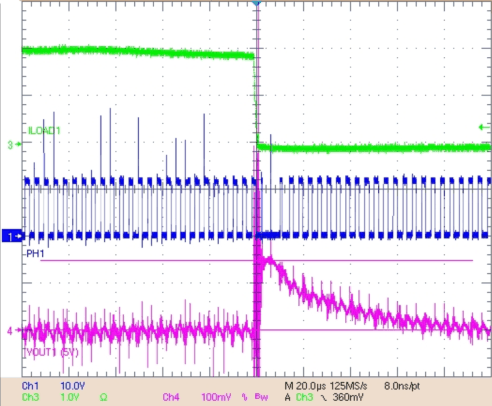 Figure 29. Load Step on VBUCK 1 From 2 A to 0 A, VOUT1 Overshoot = 148 mV
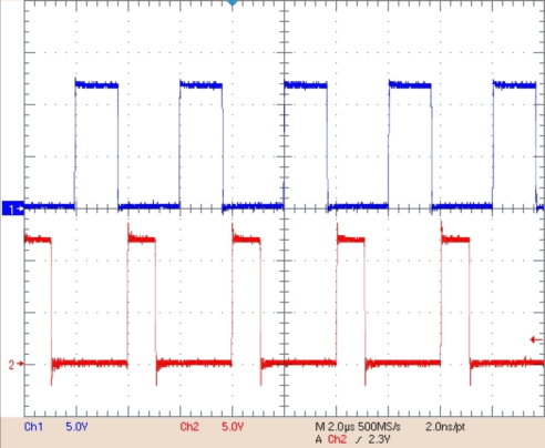 Figure 31. VBUCK 1 and VBUCK 2 Switching 180° Out of Phase
 Figure 33. VBUCK 1 Power-On Delay From Enable Going High, ∆t = 2.8 ms (ILoad = 1.3 A)
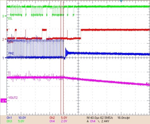 Figure 35. VBUCK 2 Turnoff Delay From I2C Enable Bit Going Low, ∆t = 7.2 µs
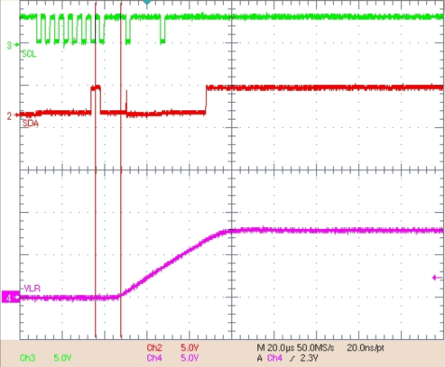 Figure 37. Linear Regulator (VLR) Turnon Delay From I2C Enable Bit Going High, ∆t = 12 µs
 Figure 39. Linear Regulator (VLR) Turnoff Delay From I2C Enable Bit Going Low, ∆t = 6.4 µs
 Figure 26. High-Side Driver (HSD) Output Power-On Delay From I2C Bit Enable, ∆t = 47 µs
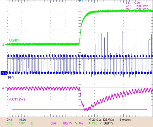 Figure 28. Load Step on VBUCK 1 From 0 A to 2 A, VOUT1 Droop = 150 mV
 Figure 30. Load Step on VBUCK 2 From 0 A to 1.3 A, VOUT1 Droop = 102 mV
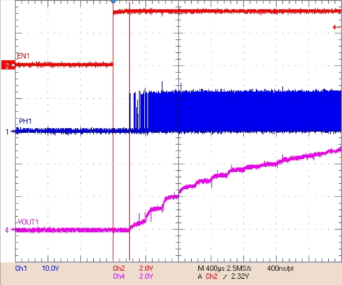 Figure 32. VBUCK 1 Turnon Delay From Enable Going High, ∆t = 200 µs
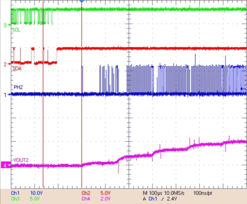 Figure 34. VBUCK 2 Turnon Delay From I2C Enable Bit Going High, ∆t = 164 µs
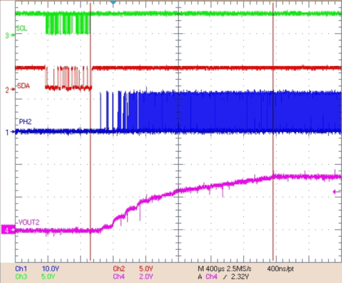 Figure 36. VBUCK 2 Power-On Delay From I2C Enable Bit Going High, ∆t = 2.24 ms
 Figure 38. Linear Regulator (VLR) Power-On Delay From I2C Enable Bit Going High, ∆t = 61.2 µs
8.3 System Example
8.3.1 Multiple Power Supply Configuration for Vehicle Audio Applications
Figure 40 shows an example of configuration for car-audio power-supply application. Other combinations are possible depending on the system requirements.
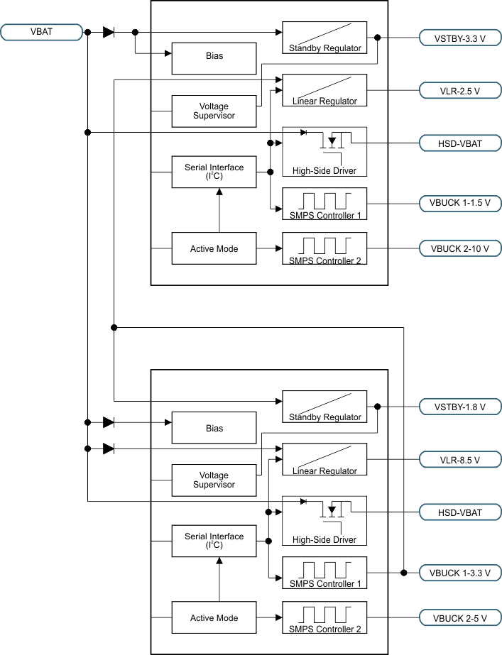 Figure 40. Multiple Power Supply for Vehicle Audio
