JAJSHA3K December 2012 – May 2019 TPS50301-HT
PRODUCTION DATA.
- 1 特長
- 2 アプリケーション
- 3 概要
- 4 改訂履歴
- 5 概要(続き)
- 6 Pin Configuration and Functions
- 7 Specifications
-
8 Detailed Description
- 8.1 Overview
- 8.2 Functional Block Diagram
- 8.3
Feature Description
- 8.3.1 VIN and Power VIN Pins (VIN and PVIN)
- 8.3.2 PVIN vs Frequency
- 8.3.3 Voltage Reference
- 8.3.4 Adjusting the Output Voltage
- 8.3.5 Maximum Duty Cycle Limit
- 8.3.6 PVIN vs Frequency
- 8.3.7 Safe Start-Up into Prebiased Outputs
- 8.3.8 Error Amplifier
- 8.3.9 Slope Compensation
- 8.3.10 Enable and Adjust UVLO
- 8.3.11 Adjustable Switching Frequency and Synchronization (SYNC)
- 8.3.12 Slow Start (SS/TR)
- 8.3.13 Power Good (PWRGD)
- 8.3.14 Bootstrap Voltage (BOOT) and Low Dropout Operation
- 8.3.15 Sequencing (SS/TR)
- 8.3.16 Output Overvoltage Protection (OVP)
- 8.3.17 Overcurrent Protection
- 8.3.18 TPS50301-HT Thermal Shutdown
- 8.3.19 Turn-On Behavior
- 8.3.20 Small Signal Model for Loop Response
- 8.3.21 Simple Small Signal Model for Peak Current Mode Control
- 8.3.22 Small Signal Model for Frequency Compensation
- 8.4 Device Functional Modes
-
9 Application and Implementation
- 9.1 Application Information
- 9.2
Typical Application
- 9.2.1 Design Requirements
- 9.2.2
Detailed Design Procedure
- 9.2.2.1 Custom Design With WEBENCH® Tools
- 9.2.2.2 Operating Frequency
- 9.2.2.3 Output Inductor Selection
- 9.2.2.4 Output Capacitor Selection
- 9.2.2.5 Input Capacitor Selection
- 9.2.2.6 Slow Start Capacitor Selection
- 9.2.2.7 Bootstrap Capacitor Selection
- 9.2.2.8 Undervoltage Lockout (UVLO) Set Point
- 9.2.2.9 Output Voltage Feedback Resistor Selection
- 9.2.2.10 Compensation Component Selection
- 9.2.3 Parallel Operation
- 9.2.4 Application Curve
- 10Power Supply Recommendations
- 11Layout
- 12デバイスおよびドキュメントのサポート
- 13メカニカル、パッケージ、および注文情報
8.3.22 Small Signal Model for Frequency Compensation
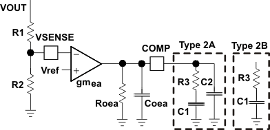
The device uses a transconductance amplifier for the error amplifier and readily supports two of the commonly used frequency compensation circuits shown in Figure 28. In Type 2A, one additional high-frequency pole is added to attenuate high-frequency noise.
The following design guidelines are provided for advanced users who prefer to compensate using the general method. The step-by-step design procedure described in Detailed Design Procedure may also be used.
 Figure 28. Types of Frequency Compensation
 The general design guidelines for device loop compensation are as follows:
- Determine the crossover frequency ƒc. A good starting point is one-tenth of the switching frequency, ƒSW.
- R3 can be determined by:
- gmea is the GM amplifier gain ( 1300 μA/V).
- gmps is the power stage gain (18 A/V).
- Vref is the reference voltage (0.795 V)
- Place a compensation zero at the dominant pole
 .
.
C1 can be determined by - C2 is optional. It can be used to cancel the zero from the equivalent series resistance (ESR) of the output capacitor Co.
Equation 17. 

where
Equation 18. 

Equation 19. 

NOTE
For PSpice models and WEBENCH design tool, see the Tools & Software tab.
- PSpice average model (stability – bode plot)
- PSpice transient model (switching waveforms)
- WEBENCH design tool www.ti.com/product/TPS50301-HT/toolssoftware