TPS51120 Dual, Synchronous Step-Down Controller With 100-mA Standby Regulators for Notebook System Power
1 Features
- 3.3-V and 5-V 100-mA Bootstrapped Standby Regulators with Independent Enables
- Selectable D-CAP™ Mode Enables Fast Transient Response Less than 100 ns
- Selectable Low Ripple Current Mode
- Less than 1% Internal Reference Accuracy
- Selectable PWM-only/Auto-skip Modes
- Low-side RDS(on) Loss-less Current Sensing
- RSENSE Accurate Current Sense Option
- Internal Soft-Start and Integrated VOUT Discharge Transistors
- Integrated 2-V Reference
- Adaptive Gate Drivers with Integrated Boost Diode
- Powergood for Each Channel with Delay Timer
- Fault Disable Mode
- Supply Input Voltage Range: 4.5 V to 28 V
2 Applications
Notebook Computers System Bus and I/O
3 Description
The TPS51120 is a highly sophisticated dual, synchronous step-down controller. It is a full featured controller designed to run directly off a three- or four-cell Li-ion battery and provide high-power and 5-V and/or 3.3-V standby regulation for all the downstream circuitry in a notebook computer system. High-current, 100-mA, 5-V or 3.3-V on-board linear regulators have glitch-free switch over function to SMPS and can be kept alive independently during standby state. The pseudo-constant frequency adaptive on-time control scheme supports full range of current mode operation including simplified loop compensation, ceramic output capacitors as well as seamless transition to reduced frequency operation at light-load condition. Optional D-CAP mode operation optimized for SP-CAP or POSCAP output capacitors allows further reduction of external compensation parts. Dynamic UVP supports VIN line sag without latch off by hitting 5-V UVP. No negative voltage appears at output voltage node during UVLO, UVP, and OCP, OTP or loss of VIN.
The TPS51120 32-pin QFN package is specified from –40°C to 85°C ambient temperature.
Device Information(1)
| PART NUMBER | PACKAGE | BODY SIZE (NOM) |
|---|---|---|
| TPS51120 | VQFN (32) | 5.00 mm × 5.00 mm |
- For all available packages, see the orderable addendum at the end of the datasheet.
Reference Design for D-CAP Mode Converter
4 Revision History
Changes from B Revision (Feburary 2007) to C Revision
- Added Pin Configuration and Functions section, Feature Description section, Device Functional Modes, Application and Implementation section, Power Supply Recommendations section, Layout section, Device and Documentation Support section, and Mechanical, Packaging, and Orderable Information section Go
5 Pin Configuration and Functions

Pin Functions
| PIN | I/O | DESCRIPTION | |
|---|---|---|---|
| NAME | NO. | ||
| COMP1 | 2 | O | Loop compensation pin (error amplifier output). Connect RC from this pin to GND for proper loop compensation with current mode operation. Tie this pin to V5FILT for D-CAP mode operation. |
| COMP2 | 7 | O | |
| CS1 | 23 | I | Current sense comparator input (-) for resistor sensing scheme. Or, overcurrent trip setting input for RDS(on) current sense scheme if connected to V5FILT through the threshold setting resistor. |
| CS2 | 18 | I | |
| DRVH1 | 27 | O | High-side MOSFET gate drive output. Source 3.5 Ω, sink 1.5 Ω, LL-node referenced floating driver. Drive voltage corresponds to VBST to LL voltage. |
| DRVH2 | 14 | O | |
| DRVL1 | 25 | O | Rectifying (low-side) MOSFET gate drive output. Source 3.5 Ω, sink 1.5 Ω, PGND referenced driver. Drive voltage is VREG5 voltage. |
| DRVL2 | 16 | O | |
| EN1 | 29 | I | Channel 1 and Channel 2 SMPS enable pins. Connect to 5 V to turn on with internal 3-ms soft-start. Slower soft-start is possible by applying an external capacitor from each of these pins to ground to program ramp rate. |
| EN2 | 12 | I | |
| EN3 | 10 | I | VREG3, 3.3-V low dropout linear regulator enable pin. Connect to GND to disable. Float or tie to enabled VREG5 to turn on the regulator. |
| EN5 | 9 | I | VREG5, 5-V low dropout linear regulator enable pin. Connect to GND to disable. Float or tie to VBAT to turn on the regulator. |
| GND | 5 | I | Signal ground pin. |
| LL1 | 26 | I/O | High-side MOSFET gate driver return. Also serve as current sense comparator input (-) for RDS(on) sensing, and input voltage monitor for on-time control circuitry |
| LL2 | 15 | I/O | |
| PGND1 | 24 | I/O | Ground return for rectifying MOSFET gate driver. Connect PGND2, PGND1 and GND strongly together near the source of the rectifying FET or the GND connection of the current sense resistor. Also serve as current sense comparator input (+). |
| PGND2 | 17 | I/O | |
| PGOOD1 | 30 | O | Power-good window comparator open drain output. Pull up with resistor to V5FILT or appropriate signal voltage. Current capability is 5-mA. PGOOD goes high 1-ms after VFB is within specified limits. Power bad (terminal goes low) is within 10 μs. |
| PGOOD2 | 11 | O | |
| SKIPSEL | 32 | I | Skip and fault mode selection pin. Refer to Table 5 |
| TONSEL | 31 | I | On-time selection pin. Refer to Table 1 and Table 5. |
| V5FILT | 20 | I | 5-V supply input for the entire control circuit. Should be provided from VREG5 via RC filter. |
| VBST1 | 28 | I | Supply Input for High-side MOSFET Driver. Connect capacitor from this pin to respective LL terminal. An internal PN diode is connected between VREG5 to each of these pins. User can add external schottky diode if forward drop is critical to drive the power MOSFET. |
| VBST2 | 13 | I | |
| VFB1 | 3 | I | SMPS feedback input. Connect the feedback resistor divider here for adjustable outputs. Tie these pins to V5FILT or for fixed output option. Refer to Table 5 |
| VFB2 | 6 | I | |
| VIN | 22 | I | Supply Input for 5-V and 3.3-V linear regulator. Typically connected to VBAT. |
| VO1 | 1 | I | These terminals serve four functions: on-time adjustment, output discharge, VREG5, VREG3 switchover input and feedback inputs for 5-V, 3.3-V fixed-output option. Connect to positive terminal of respective switch mode power supply’s output capacitor. |
| VO2 | 8 | I | |
| VREF2 | 4 | O | 2-V reference output. Capable of ±50-μA, ±2% over 0 - 85°C temperature range. Bypass to GND by 1-nF ceramic capacitor. Tie this pin to GND disables both SMPS. |
| VREG3 | 19 | O | 3.3-V, 100-mA low dropout linear regulator output. Bypass to PGND by 10-μF ceramic capacitor. Runs from VIN supply. Shuts off with EN3. Switches over to VO2 when 3.1 V or above is provided. |
| VREG5 | 21 | O | 5-V, 100-mA low dropout linear regulator output. Bypass to PGND by 10-μF ceramic capacitor. Runs from VIN supply. Internally connected to VBST and DRVL. Shuts off with EN5. Switches over to VO1 when 4.8 V or above is provided. |
6 Specifications
6.1 Absolute Maximum Ratings
over operating free-air temperature range unless otherwise noted(1)| MIN | MAX | UNIT | |||
|---|---|---|---|---|---|
| Input voltage | VBST1, VBST2 | –0.3 | 36 | V | |
| VBST1, VBST2 wrt LL | –0.3 | 6 | |||
| VIN, EN5 | –0.3 | 30 | |||
| SKIPSEL, TONSEL, EN1, EN2, CS1, CS2, V5FILT, VFB1, VFB2, EN3, VO1, VO2 | –0.3 | 6 | |||
| Output voltage | DRVH1, DRVH2 | –1 | 36 | V | |
| DRVH1, DRVH2 (wrt LL) | –0.3 | 6 | |||
| LL1, LL2 | –1 | 30 | |||
| VREF2, VREG3, VREG5, PGOOD1, PGOOD2, DRVL1, DRVL2, COMP1, COMP2 | –0.3 | 6 | |||
| PGND1, PGND2 | –0.3 | 0.3 | |||
| Source/sink current | VREF2 | 1 | mA | ||
| VBST | 100 | ||||
| VREG5, VREG3 (source only) | 200 | ||||
| TA | Operating ambient temperature | –40 | 85 | °C | |
| TJ | Junction temperature | –40 | 125 | ||
| Lead temperature 1.6 mm (1/16 inch) from case for 10 seconds | 255 | ||||
| Tstg | Storage temperature | –55 | 150 | ||
6.2 Recommended Operating Conditions
| MIN | MAX | UNIT | ||
|---|---|---|---|---|
| Input voltage, V5FILT | 4.5 | 5.5 | V | |
| Input voltage range | VBST1, VBST2 | -0.1 | 34 | V |
| VBST1, VBST2 wrt LL | -0.1 | 5.5 | ||
| VIN, EN5 | -0.1 | 28 | ||
| SKIPSEL, TONSEL, EN1, EN2, CS1, CS2, V5FILT, VFB1, VFB2, EN3 | -0.1 | 5.5 | ||
| VO1, VO2 | -0.1 | 5.5 | ||
| Output voltage range | DRVH1, DRVH2 | -0.8 | 34 | V |
| DRVH1, DRVH2 (wrt LL) | -0.1 | 5.5 | ||
| LL1, LL2 | -0.8 | 28 | ||
| VREF2, VREG5, VREG3, PGOOD1, PGOOD2, DRVL1, DRVL2, COMP1, COMP2 | -0.1 | 5.5 | ||
| PGND1, PGND2 | -0.1 | 0.1 | ||
| Source/sink current | VREF2 | 0.08 | mA | |
| VBST | 50 | |||
| VREG5, VREF3 (source only) | 100 | |||
| Operating ambient temperature range, TA | -40 | 85 | °C | |
6.3 Thermal Information
| THERMAL METRIC(1) | TPS51120 | UNIT | |
|---|---|---|---|
| RHB | |||
| 32 PINS | |||
| RθJA | Junction-to-ambient thermal resistance | 38.5 | °C/W |
6.4 Electrical Characteristics
over operating free-air temperature range, VVIN = 12 V, VVREG5 = VV5FILT = 5 V (unless otherwise noted)| PARAMETER | TEST CONDITIONS | MIN | TYP | MAX | UNIT | ||
|---|---|---|---|---|---|---|---|
| SUPPLY CURRENT | |||||||
| IINCCAP | Supply current | VIN current, VREG5=VREG3=No Load, EN3=EN5=FLOAT, EN1=EN2=5V, CS=5V, COMP connected to Cap | Current mode | 750 | 1500 | μA | |
| IINNOCAP | Supply current | VIN current, VREG5=VREG3=No Load, EN3=EN5=FLOAT; EN1=EN2=5V, CS=5V, COMP=5V | D-CAP mode | 700 | 1400 | ||
| IIN5(STBY) | Stand-by current | VIN current, VREG5=No Load EN3=0V, EN5=FLOAT, EN1=EN2=0 | 5-V only | 30 | 45 | ||
| IIN3(STBY) | Stand-by current | VIN current, VREG3=No Load EN3=FLOAT, EN5=0, EN1=EN2=0 | 3.3-V only | 12 | 20 | ||
| IIN532(STBY) | Stand-by current | VIN current, VREG5=VREG3=VREF2=No Load EN3=EN5=FLOAT, EN1=EN2=0 | 100 | 160 | |||
| IIN(SHDN) | Shut down current | VIN current, EN3=EN5=EN1=EN2=0V | 10 | 20 | |||
| VOUT and VREF2 VOLTAGES | |||||||
| VOUT | Output voltage | VFB2 = 3.3 V, TA= 25°C, No Load | 3.241 | 3.300 | 3.359 | V | |
| VFB2 = 3.3 V, TA= 0 to 85°C, No Load | 3.234 | 3.300 | 3.366 | ||||
| VFB2 = 3.3 V, TA= -40 to 85°C, No Load | 3.224 | 3.300 | 3.376 | ||||
| VFB1 = 5 V, TA= 25°C, No Load | 4.910 | 5.000 | 5.090 | ||||
| VFB1 = 5 V, TA= 0 to 85°C, No Load | 4.900 | 5.000 | 5.100 | ||||
| VFB1 = 5 V, TA= -40 to 85°C, No Load | 4.885 | 5.000 | 5.115 | ||||
| Adjustable mode output range | 1.0 | 5.5 | |||||
| VADJ | Output regulation voltage | Adjustable mode | 1.00 | V | |||
| VADJ T | Output regulation voltage tolerance | Adjustable mode, TA= 25°C | -0.9% | 0.9% | |||
| Adjustable mode, TA= 0 to 85°C | -1.3% | 1.3% | |||||
| Adjustable mode, TA= -40 to 85°C | -1.6% | 1.6% | |||||
| VVREF2 | 2-V output regulation voltage | IVREF2 ± 50 μA, TA= 25°C | 1.97 | 2.00 | 2.03 | V | |
| VVREF2T | 2-V output regulation voltage tolerance | IVREF2 ± 50 μA, TA= 0 to 85°C | 1.96 | 2.04 | |||
| IVREF2 ± 50 μA, TA= -40 to 85°C | 1.95 | 2.05 | |||||
| IVFB | VFB input current | VFBx=1.02V, COMPx=open | 0.02 | μA | |||
| VFBx=1.02V, COMPx=5V | 0.02 | ||||||
| RDISCHARG | Discharge switch resistance | VOx=0.5V, TA= 25°C | 10 | 20 | Ω | ||
| VREG3 VOLTAGE | |||||||
| VVREG3 | VREG3 Output Regulation Voltage | IVREG3 = 20 mA, 6V < VIN < 28V, TA= 25°C | 3.25 | 3.30 | 3.35 | V | |
| VVREG3T | VREG3 Output Voltage Tolerance | IVREG3 = 1 - 50 mA , 6V < VIN < 28V, TA= 0 to 85°C | 3.21 | 3.37 | |||
| IVREG3 = 1 - 100 mA , 6V < VIN < 28V, TA= -40 to 85°C | 3.16 | 3.39 | |||||
| IVREG3 | VREG3 Output Current | TA = 25°C, VREG3=3.14V(1) | 170 | mA | |||
| VLDO3SW | VREG3 Bootstrap Switch Threshold | Rising edge of VO2, VREG3 drops to VO2 voltage | 2.85 | 3.10 | V | ||
| Hysteresis | 120 | mV | |||||
| RLDO3SW | VREG3 Bootstrap Switch Resistance | 1.3 | 3.0 | Ω | |||
| VREG5 VOLTAGE | |||||||
| VVREG5 | VREG5 Output Regulation Voltage | IVREG5 = 20 mA, 6V < VIN < 28V, TA= 25°C | 4.925 | 5.00 | 5.075 | V | |
| VVREG5T | VREG5 Output Voltage Tolerance | IVREG5 = 1 - 50 mA , 6V < VIN < 28V, TA= 0 to 85°C | 4.89 | 5.11 | |||
| IVREG5 = 1 - 100 mA , 6V < VIN < 28V, TA= -40 to 85°C | 4.80 | 5.15 | |||||
| IVREG5 | VREG5 Output Current | TA = 25°C, VREG5=4.75 V(1) | 200 | mA | |||
| VLDO5SW | VREG5 Bootstrap Switch Threshold | Rising edge of VO1, VREG5 drops to VO1 voltage | 4.30 | 4.85 | V | ||
| Hysteresis | 140 | mV | |||||
| RLDO5SW | VREG5 Bootstrap Switch Resistance | 1.3 | 3.0 | Ω | |||
| TRANSCONDUCTANCE AMPLIFIER | |||||||
| Gm | Gain | TA = 25°C | 280 | μS | |||
| ICOMPSINK | COMP Maximum Sink Current | VFBx=1.05V, COMPx=1.28V | 8 | 12 | 16 | μA | |
| ICOMPSRC | COMP Maximum Source Current | VFBx=0.95V, COMPx=1.28V | -15 | -11 | -7 | ||
| VCOMPHI | COMP High Clamp Voltage | CSx=0V, VFBx=0.95V | 1.26 | 1.34 | 1.42 | V | |
| VCOMPLO | COMP Low Clamp Voltage | CSx=0V, VFBx=1.05V | 1.08 | 1.12 | 1.20 | ||
| OUTPUT DRIVER | |||||||
| RDRVH | DRVH resistance | Source, VVBST-DRVH = 1V | 3.5 | 7 | Ω | ||
| Sink, VDRVH-LL = 1V | 1.5 | 3 | |||||
| RDRVL | DRVL resistance | Source, VVREG5-DRVL = 1V | 3.5 | 7 | |||
| Sink, VDRVL-PGND = 1V | 1.5 | 3 | |||||
| TD | Dead time | DRVH-off to DRVL-on, TA= 25°C | 20 | ns | |||
| DRVL-off to DRVH-on, TA= 25°C | 30 | 60 | |||||
| VDTH | DRVH-off threshold | LL to GND(1) | 2 | V | |||
| VDTL | DRVL-off threshold | DRVL to GND (1) | 1.1 | ||||
| INTERNAL BST DIODE | |||||||
| VFBST | Forward Voltage | VVREG5-VBST, IF = 10 mA, TA= 25°C | 0.7 | 0.8 | 0.9 | V | |
| IRBST | Reverse Current | VBST = 34 V, VREG5=5V | 0.1 | 1.0 | μA | ||
| IBST(LEAK) | VBST Leakage current | VBST=34V, LL=28V, EN3=EN5=EN1=EN2=0V | 0.1 | 1.0 | |||
| ON-TIME TIMER, INTERNAL SOFT-START and HOUSEKEEPING CLOCK | |||||||
| TON1a | On time, 5V, 180 kHz | VLL1=12V, VOUT1=5V, TONSEL=5V, TA= 25°C | 2150 | 2340 | 2530 | ns | |
| TON1b | On time, 5V, 220 kHz | VLL1=12V, VOUT1=5V, TONSEL=FLOAT, TA= 25°C | 1790 | 1950 | 2110 | ||
| TON1c | On time, 5V, 280 kHz | VLL1=12V, VOUT1=5V, TONSEL=2V, TA= 25°C | 1370 | 1490 | 1610 | ||
| TON1d | On time, 5V, 380 kHz | VLL1=12V, VOUT1=5V, TONSEL=GND, TA= 25°C | 1020 | 1110 | 1200 | ||
| TON2a | On time, 3.3V, 270 kHz | VLL2=12V, VOUT2=3.3V, TONSEL=5V, TA= 25°C | 940 | 1030 | 1120 | ||
| TON2b | On time, 3.3V, 330 kHz | VLL2==12V, VOUT1=3.3V, TONSEL=FLOAT, TA= 25°C | 780 | 850 | 920 | ||
| TON2c | On time, 3.3V, 430 kHz | VLL2==12V, VOUT1=3.3V, TONSEL=2V, TA= 25°C | 580 | 650 | 720 | ||
| TON2d | On time, 3.3V, 580 kHz | VLL2==12V, VOUT1=3.3V, TONSEL=GND, TA= 25°C | 430 | 480 | 530 | ||
| TON(MIN)1 | Minimum on time, 5V | TA = 25°C, TONSEL=GND, VLL1=28V, VO1=1V | 70 | ||||
| TON(MIN)2 | Minimum on time, 3.3V | TA = 25°C, TONSEL=GND, VLL2=28V, VO2=1V | 45 | ||||
| TOFF(MIN) | Minimum off time | TA = 25°C, VFB=0.9V, LL=0.5V | 480 | ||||
| TSS | Internal Soft Start Timer | TA = 25°C, ENx>3V | 772 | clks | |||
| SLSS | Internal Soft Start Slope | TA = 25°C, ENx>3V, Slope wrt. VFB(1) | 0.3 | V/ms | |||
| FCLK | HK clock frequency | 230 | 290 | 350 | kHz | ||
| UVLO/LOGIC THRESHOLD | |||||||
| VENLDOH | LDO enable threshold | EN3, EN5, low to high | 0.3 | 0.6 | 0.8 | V | |
| Hysteresis | 0.2 | ||||||
| VENLDOFL3 | EN3 pullup voltage | EN3 = FLOAT (OPEN)(1) | 1.7 | ||||
| VENLDOFL5 | EN5 pullup voltage | EN5= FLOAT (OPEN)(1) | 3.3 | ||||
| IENLDOFL | EN3, EN5 pullup current | VENx < 0.5V | 1.5 | 4.0 | μA | ||
| VUV(VREG5) | VREG5 UVLO threshold | Wake up | 3.8 | 4.0 | 4.2 | V | |
| Hysteresis | 100 | 200 | 300 | mV | |||
| VSKIPSEL | SKIPSEL threshold | Auto-SKIP Mode Enabled | 0 | 0.7 | V | ||
| Auto-SKIP Mode Enabled, Faults Off | 1.3 | 2.2 | |||||
| PWM-Only Mode Enabled | 2.7 | 5.5 | |||||
| VTONSEL | TONSEL threshold | Fast Switching Frequency | 0 | 0.7 | |||
| Medium Switching Frequency #2 | 1.3 | 2.2 | |||||
| Medium Switching Frequency #1 | 2.7 | 3.0 | |||||
| Slow Switching Frequency | 4.5 | 5.5 | |||||
| ISEL | SKIPSEL/TONSEL input current | SKIPSEL, TONSEL=0V | 1 | 3 | μA | ||
| SKIPSEL, TONSEL=5V | 1 | 2 | |||||
| VENSWSTAT | EN1, EN2 SS Start Voltage | BJT Base input, Switcher begins to Track ENx | 0.5 | 0.9 | 1.2 | V | |
| VENSWEND | EN1, EN2 SS End Voltage | ‘Logic High’ Level for Switcher Enable when using Internal Softstart, 0°C ≤ TA ≤ 85°C | 2.75 | 2.90 | |||
| IENSW1,2 | EN1, EN2 Pullup Current | EN1, EN2=0.6V | 1 | 2 | 3 | μA | |
| VTHVFB1 | VFB1 threshold | 5.0V preset output | V5FILT -0.3 | V | |||
| VTHVFB2 | VFB2 threshold | 3.3V preset output | V5FILT -0.3 | ||||
| CURRENT SENSE | |||||||
| VOCL | Current limit threshold | Resistor sense scheme , VPGND - VCS voltage, PGOOD=Hi | 67 | 80 | 93 | mV | |
| ITRIP | CS Sink Current | RDS(ON) sense scheme, PGOOD=Hi, TA= 25°C | 9 | 10 | 11 | μA | |
| TCITRIP | ITRIP temperature Coefficient | RDS(ON) sense scheme, On the basis of 25°C | 4500 | ppm/°C | |||
| VOCLoff | OCP Comparator Offset | (VVREG5-CS-VPGND-LL) voltage, VVREG5-CS = 80mV, RDS(ON) sense |
-10 | 0 | 10 | mV | |
| VR(trip) | Current limit threshold setting range | VV5FILT-VCS voltage | 30 | 150 | |||
| VZC | Zero cross detection Comparator offset | VPGNDx-VLLx voltage, SKIPSEL=0V | -5 | 1 | 5 | ||
| POWERGOOD COMPARATOR | |||||||
| VTH(PG) | PGOOD Threshold | Power Bad Threshold | ±7% | ±10% | ±13% | ||
| Hysteresis | ±5% | ||||||
| IPG(MAX | PGOOD Sink Current | PGOOD=0.5 V | 2.5 | 5.0 | mA | ||
| TPGDEL | PGOOD Delay Timer | Delay for PGOOD in, ‘clks’=HK Clock | 256 | clks | |||
| UNDERVOLTAGE and OVERVOLTAGE PROTECTION | |||||||
| VOVP | VFBx OVP Trip Threshold | OVP detect | 110% | 115% | 120% | ||
| TOVPDEL | VFBx OVP Delay Time | 2 | ms | ||||
| VUVP | VFBx UVP Trip Threshold | UVP detect | 65% | 70% | 75% | ||
| Hysteresis | 6% | ||||||
| TUVPDEL | VFBx UVP Delay Timer | ‘clks’=HK Clock | 128 | clks | |||
| THERMAL SHUTDOWN | |||||||
| TSDN1 | Thermal shutdown threshold | Shutdown temperature | 145 | °C | |||
| Hysteresis | 10 | ||||||
6.5 Typical Characteristics
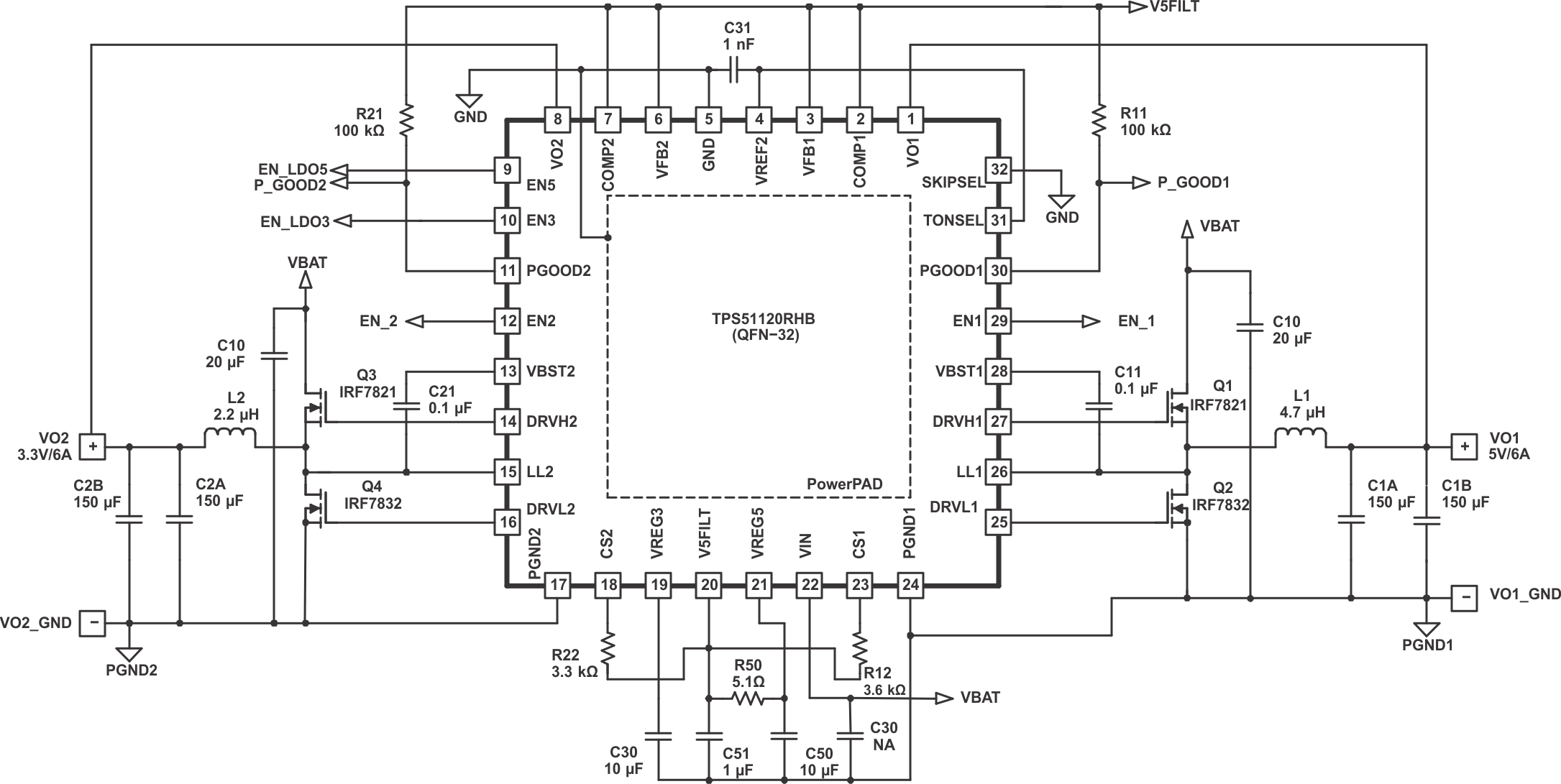
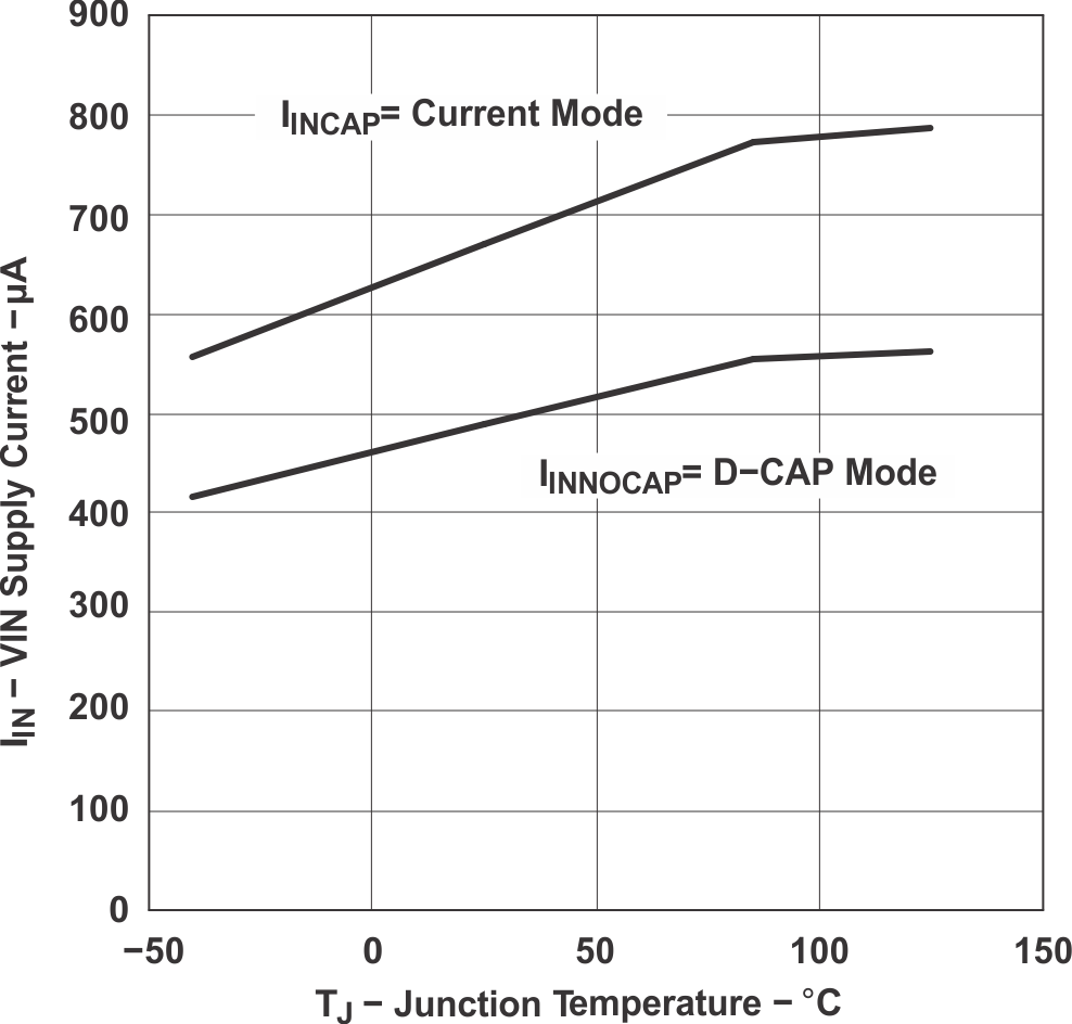 Figure 1. VIN Supply Current vs Junction Temperature
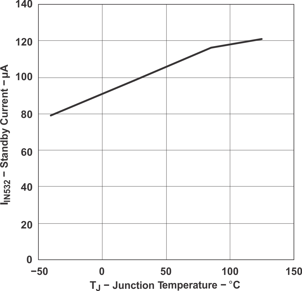 Figure 3. VIN Standby Current vs Junction Temperature
 Figure 5. VIN Shutdown Current vs Junction Temperature
 Figure 7. No-Load Battery Current vs Input Voltage
 Figure 9. Switching Frequency vs Input Voltage
 Figure 11. Switching Frequency vs Input Voltage
 Figure 13. Switching Frequency vs Output Current
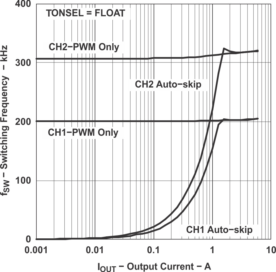 Figure 15. Switching Frequency vs Output Current
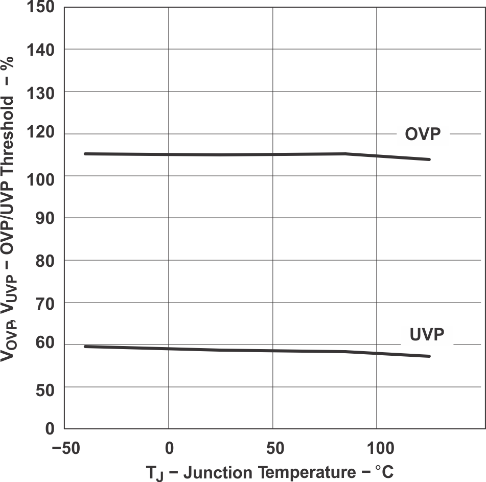 Figure 17. OVP/UVP Threshold Voltage vs Junction Temperature
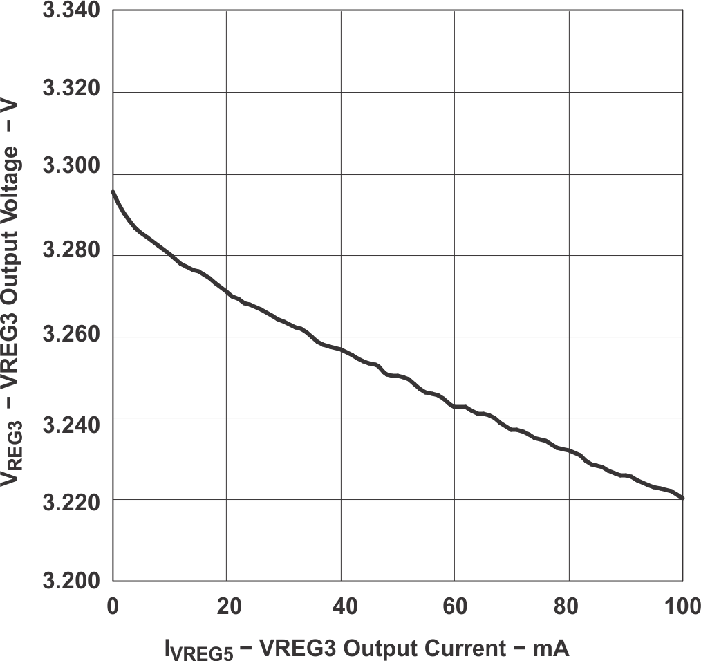 Figure 19. VREG3 Output Voltage vs Output Current
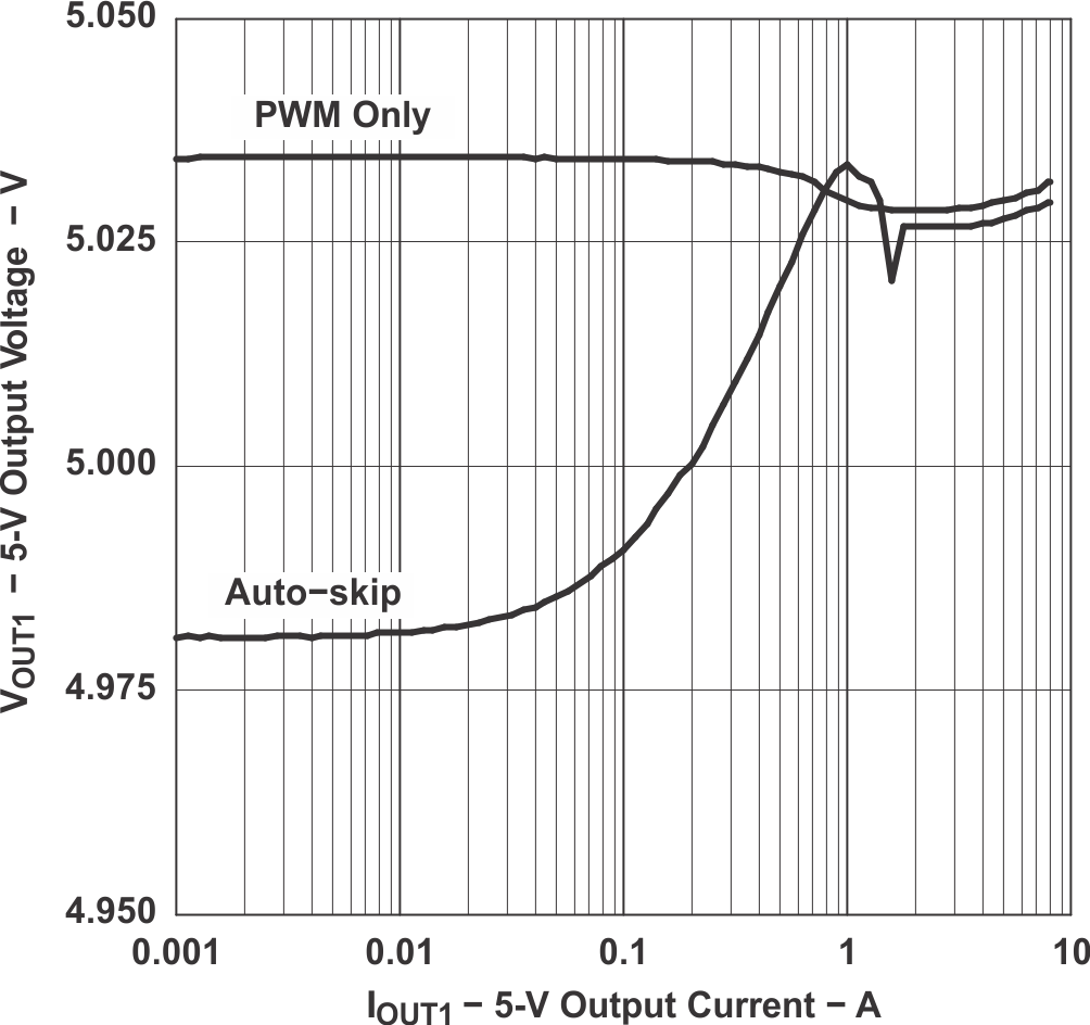 Figure 21. 5-V Output Voltage vs Output Current
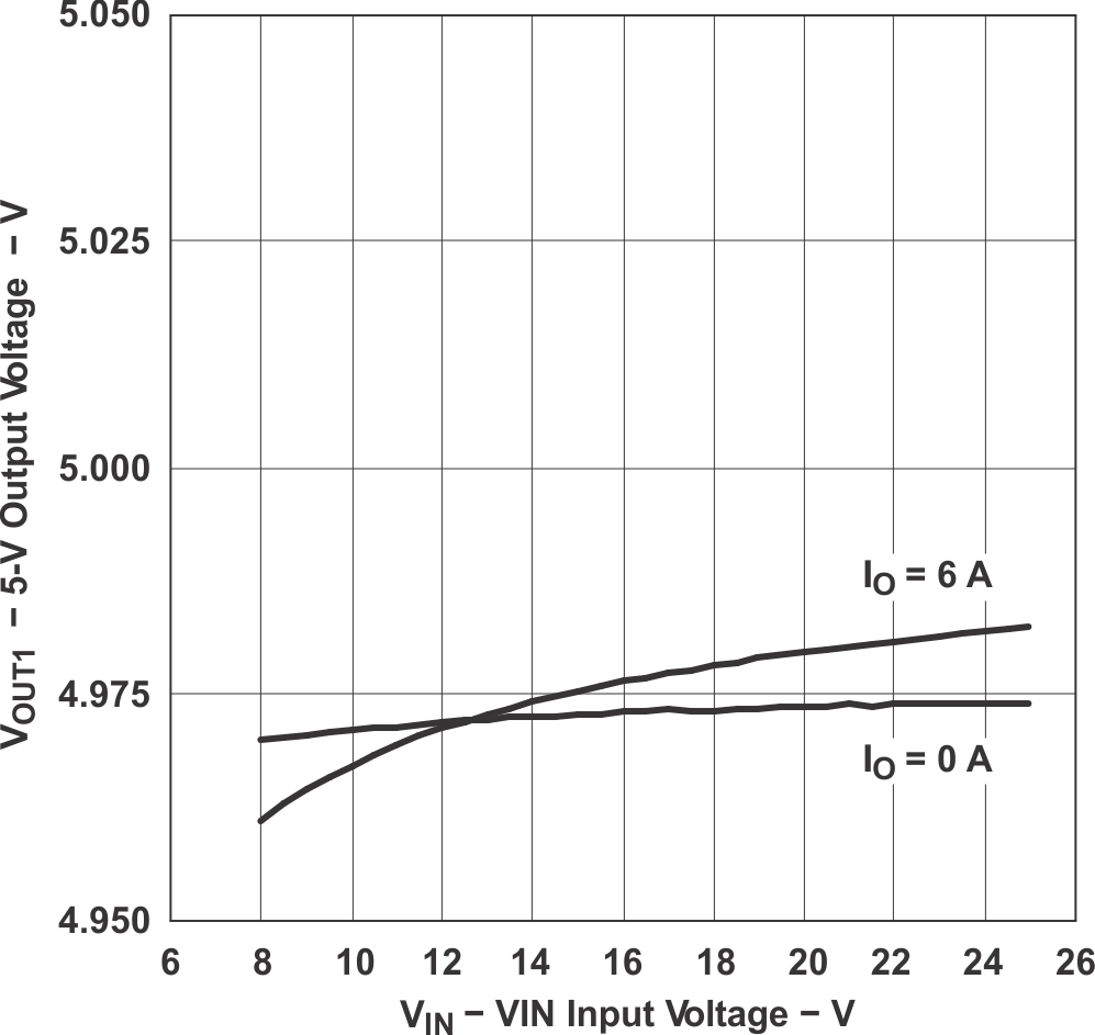 Figure 23. 5-V Output Voltage vs Input Voltage
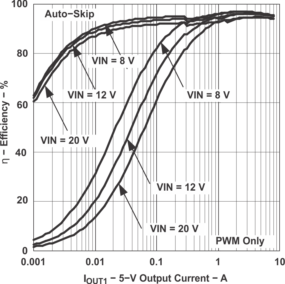 Figure 25. 5-V Efficiency vs Output Current
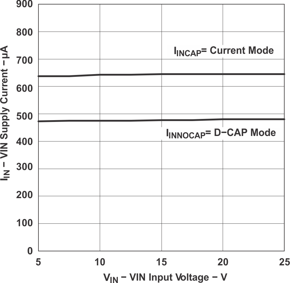 Figure 2. VIN Supply Current vs Input Voltage
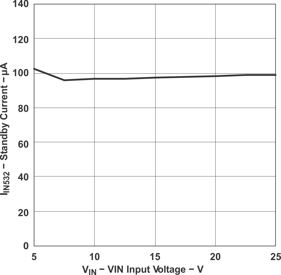 Figure 4. VIN Standby Current vs Input Voltage
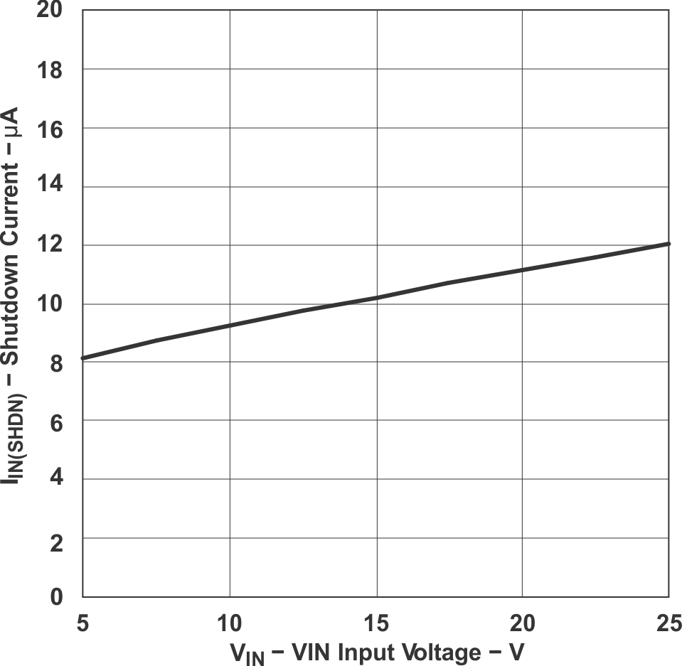 Figure 6. VIN Shutdown Current vs Input Voltage
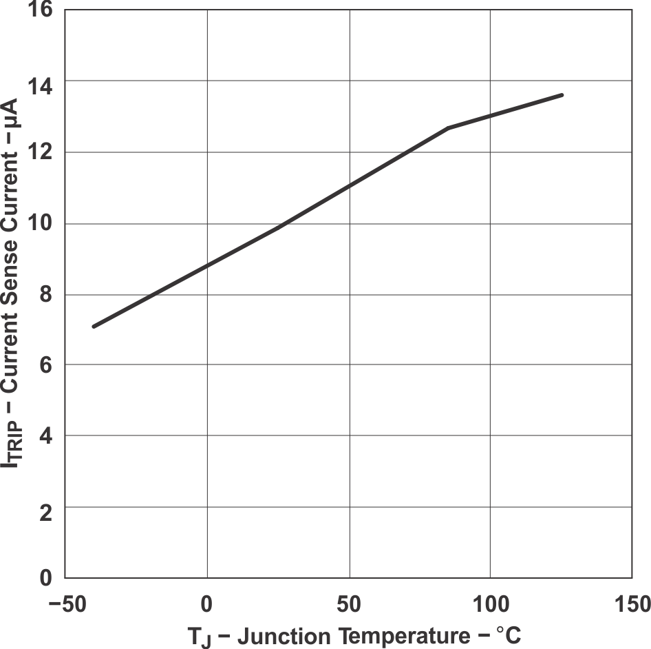 Figure 8. Current Sense Current vs Junction Temperature
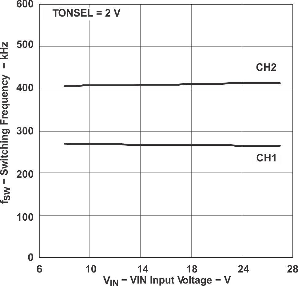 Figure 10. Switching Frequency vs Input Voltage
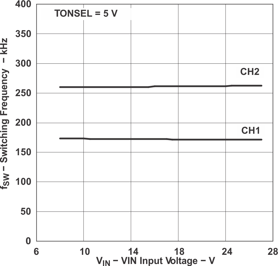 Figure 12. Switching Frequency vs Input Voltage
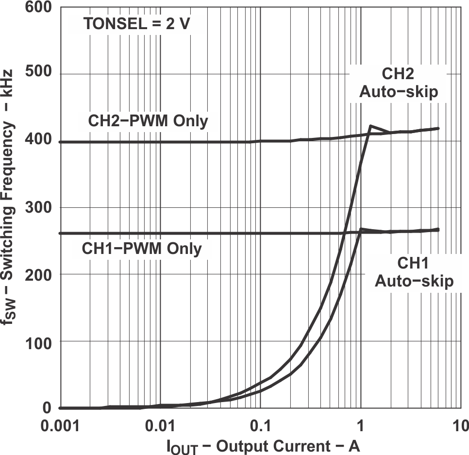 Figure 14. Switching Frequency vs Output Current
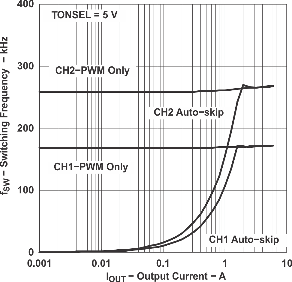 Figure 16. Switching Frequency vs Output Current
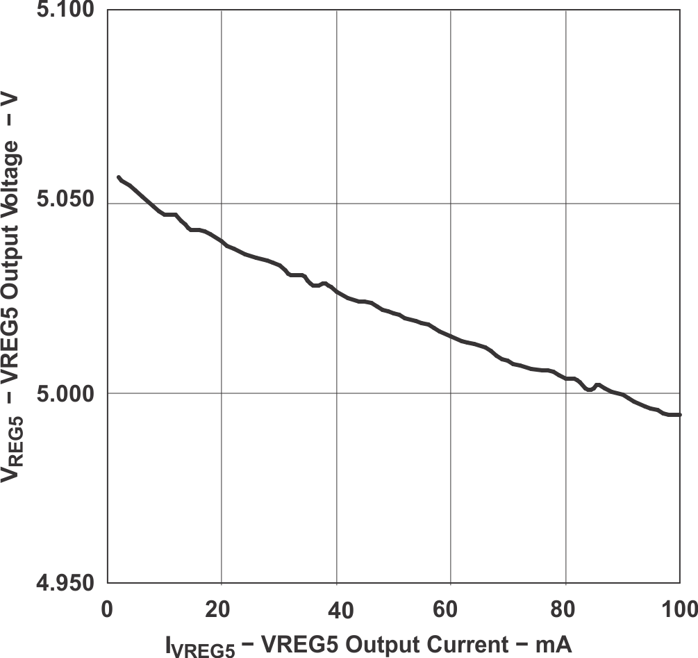 Figure 18. VREG5 Output Voltage vs Output Current
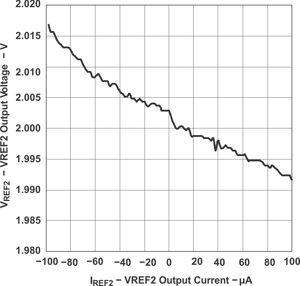 Figure 20. VREF2 Output Voltage vs Output Current
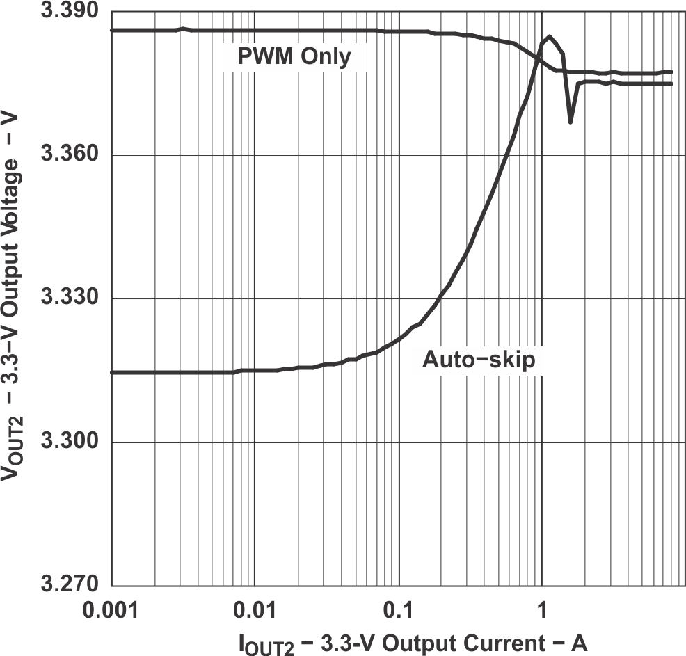 Figure 22. 3.3-V Output Voltage vs Output Current
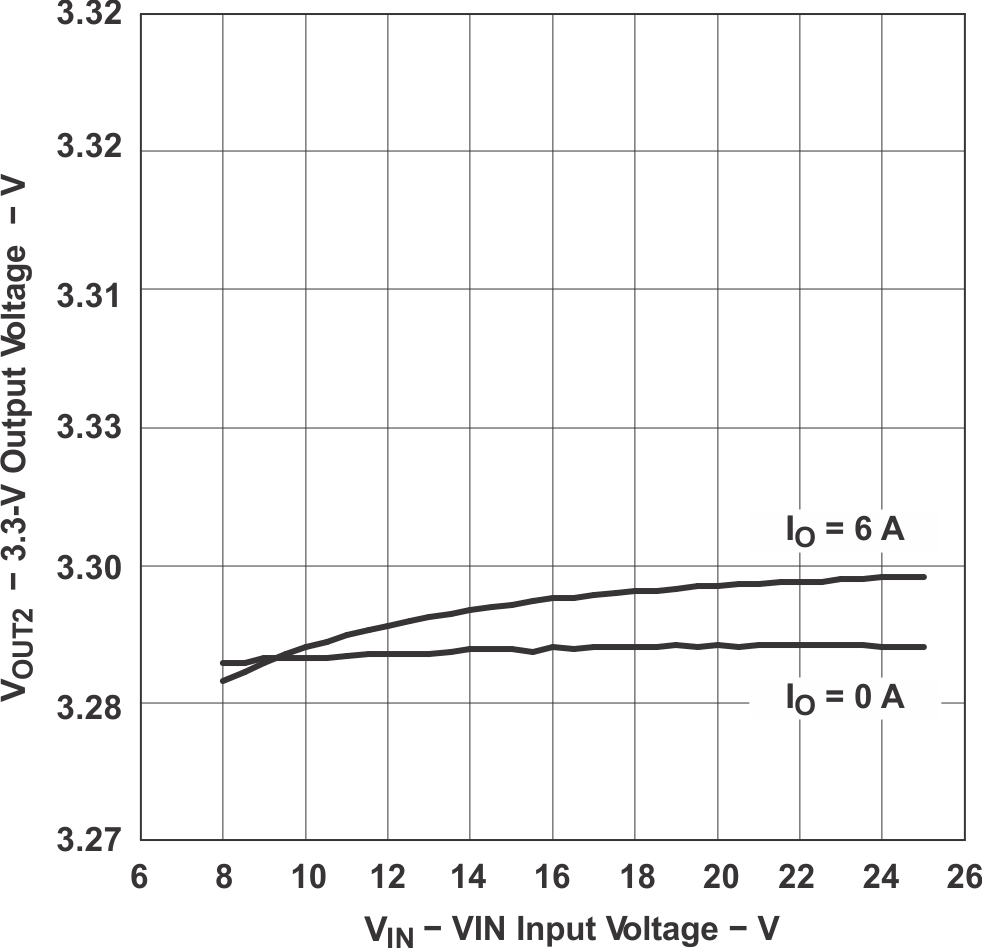 Figure 24. 3.3-V Output Voltage vs Input Voltage
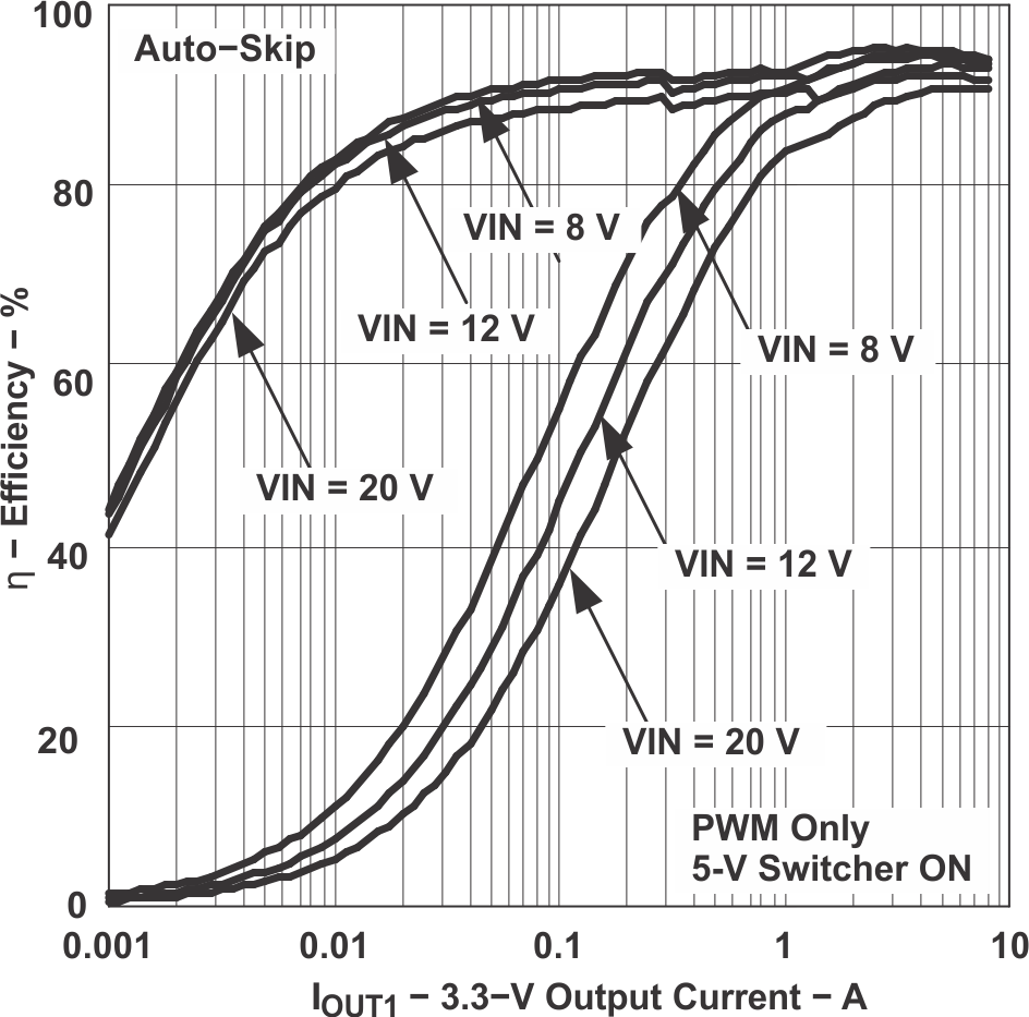 Figure 26. 3.3-V Efficiency vs Output Current