JAJSOE8A November 2015 – July 2022 TPS51216-EP
PRODUCTION DATA
- 1 特長
- 2 アプリケーション
- 3 概要
- 4 Revision History
- 5 概要 (続き)
- 6 Pin Configuration and Functions
- 7 Specifications
- 8 Detailed Description
- 9 Application and Implementation
- 10Power Supply Recommendations
- 11Layout
- 12Device and Documentation Support
- 13Mechanical, Packaging, and Orderable Information
パッケージ・オプション
メカニカル・データ(パッケージ|ピン)
- RUK|20
サーマルパッド・メカニカル・データ
- RUK|20
発注情報
9.1.3 VTT and VTTREF
TPS51216-EP integrates two high performance, low-dropout linear regulators, VTT and VTTREF, to provide complete DDR2/DDR3/DDR3L power solutions. The VTTREF has a 10-mA sink/source current capability, and tracks ½ of VDDQSNS with ±1% accuracy using an on-chip ½ divider. A 0.22-μF (or larger) ceramic capacitor must be connected close to the VTTREF terminal for stable operation. The VTT responds quickly to track VTTREF within ±40 mV at all conditions, and the current capability is 2 A for both sink and source. A 10-μF (or larger) ceramic capacitor must be connected close to the VTT terminal for stable operation. To achieve tight regulation with minimum effect of wiring resistance, a remote sensing terminal, VTTSNS, should be connected to the positive node of the VTT output capacitors as a separate trace from the high-current line to the VTT pin. (Refer to Section 11.1 for details.)
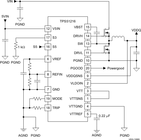
When VTT is not required in the design, the following treatments are strongly recommended.
- Connect VLDOIN to VDDQ.
- Tie VTTSNS to VTT, and remove capacitors from VTT to float.
- Connect VTTGND to GND.
- Select MODE 0 or MODE 1 shown in Table 8-2 (select non-tracking discharge mode).
- Maintain a 0.22-µF capacitor connected at VTTREF.
- Pull down S3 to GND with 1-kΩ resistance.
 Figure 9-3 Application Circuit When VTT is not Required