JAJSK76 September 2022 TPS51383
PRODUCTION DATA
- 1 特長
- 2 アプリケーション
- 3 概要
- 4 Revision History
- 5 Pin Configuration and Functions
- 6 Specifications
-
7 Detailed Description
- 7.1 Overview
- 7.2 Functional Block Diagram
- 7.3
Feature Description
- 7.3.1 PWM Operation and D-CAP3 Control Mode
- 7.3.2 VCC LDO
- 7.3.3 Soft Start
- 7.3.4 Enable Control
- 7.3.5 Power Good
- 7.3.6 Overcurrent Protection and Undervoltage Protection
- 7.3.7 100-mA LDO with Switch Over
- 7.3.8 UVLO Protection
- 7.3.9 Overvoltage Protection
- 7.3.10 Output Voltage Discharge
- 7.3.11 Thermal Shutdown
- 7.4 Device Functional Modes
- 8 Application and Implementation
- 9 Device and Documentation Support
- 10Mechanical, Packaging, and Orderable Information
6.6 Typical Characteristics
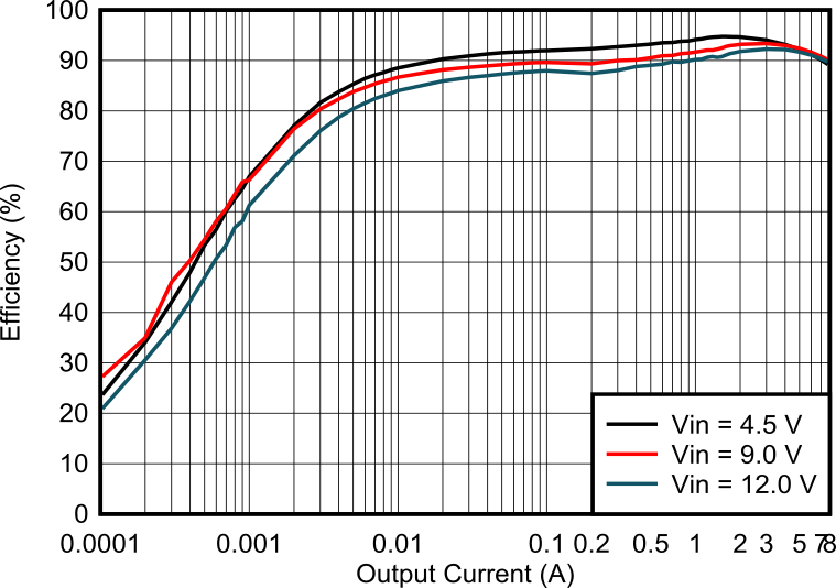
Figure 6-1 TPS51383 PSM Efficiency
 Figure 6-3 TPS51384 PSM Efficiency
Figure 6-5 TPS51383 Load Regulation
Figure 6-7 TPS51383 Fsw vs Iout
Figure 6-9 Quiescent Current vs Temperature
Figure 6-11 Enable On Voltage vs Temperature
Figure 6-13 High-side RDS(on) vs Temperature
Figure 6-15 Valley Current Limit vs Temperature
Figure 6-2 TPS51383 OOA Efficiency
Figure 6-4 TPS51384 OOA Efficiency
Figure 6-6 TPS51384 Load Regulation
Figure 6-8 TPS51384 Fsw vs Iout
Figure 6-10 Output Voltage vs
Temperature
Figure 6-12 Enable Off Voltage vs Temperature
Figure 6-14 Low-side RDS(on) vs Temperature
Figure 6-16 Soft-Start Time vs
Temperature