JAJSOS7 august 2023 TPS51385
PRODUCTION DATA
- 1
- 1 特長
- 2 アプリケーション
- 3 概要
- 4 Revision History
- 5 Pin Configuration and Functions
- 6 Specifications
- 7 Detailed Description
- 8 Application and Implementation
- 9 Device and Documentation Support
- 10Mechanical, Packaging, and Orderable Information
8.2.3 Application Curves
VIN = 19.5 V, Ta = 25°C unless otherwise specified.
 Figure 8-2 Efficiency, PSM Mode
 Figure 8-4 Switching Frequency, PSM Mode
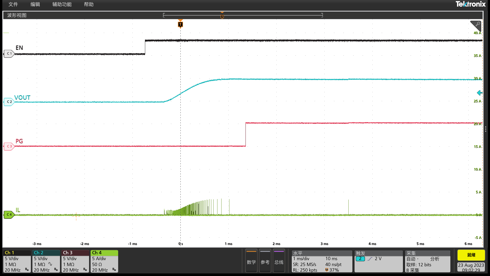 Figure 8-6 Start-Up Relative to EN Rising, Iout = 0A, PSM Mode
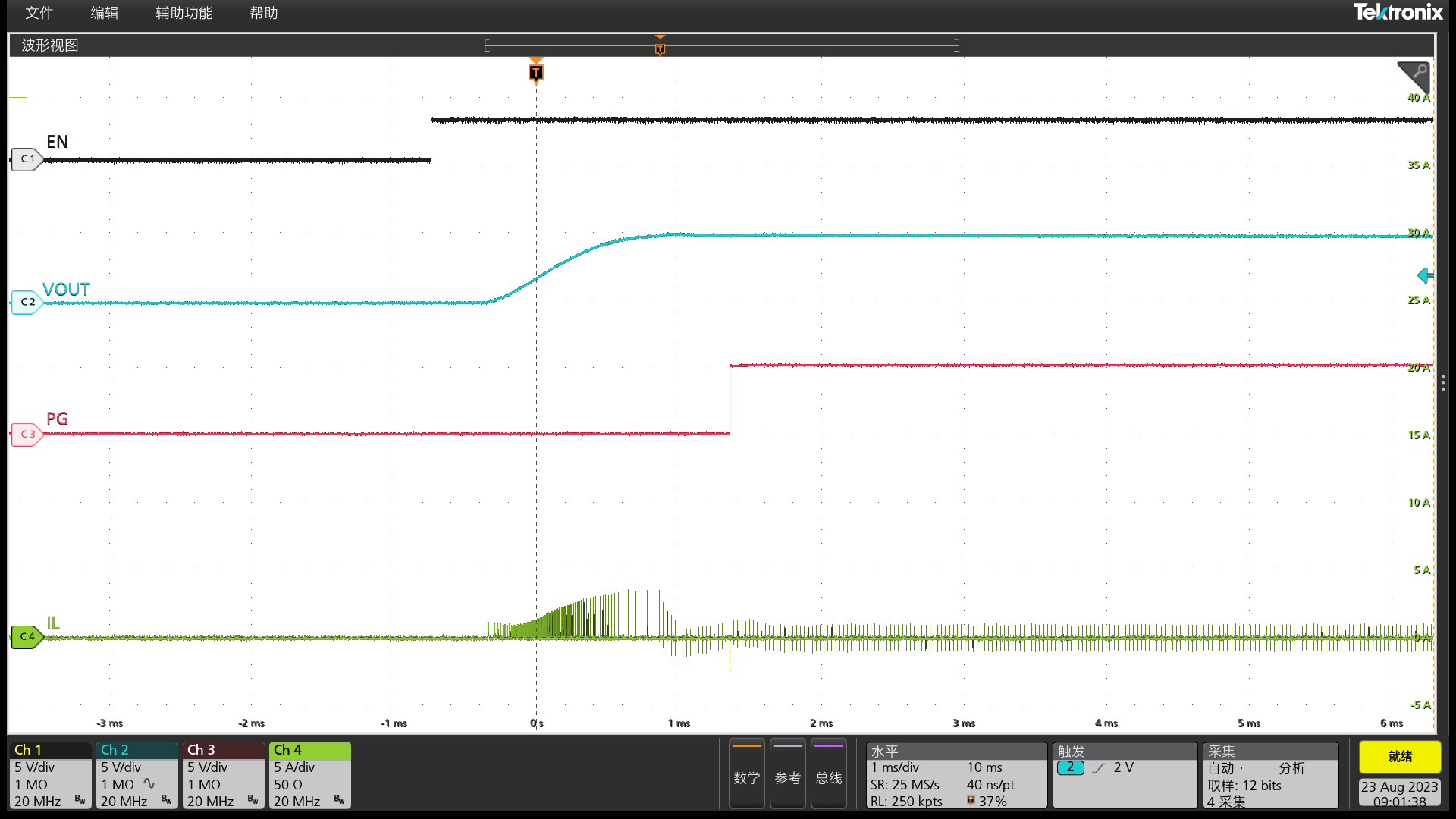 Figure 8-8 Start-Up Relative to EN
Rising, Iout = 0A, OOA Mode
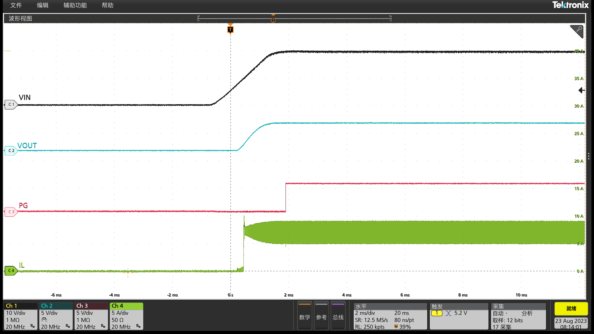 Figure 8-10 Start-Up Relative to Vin Rising, Iout = 7A
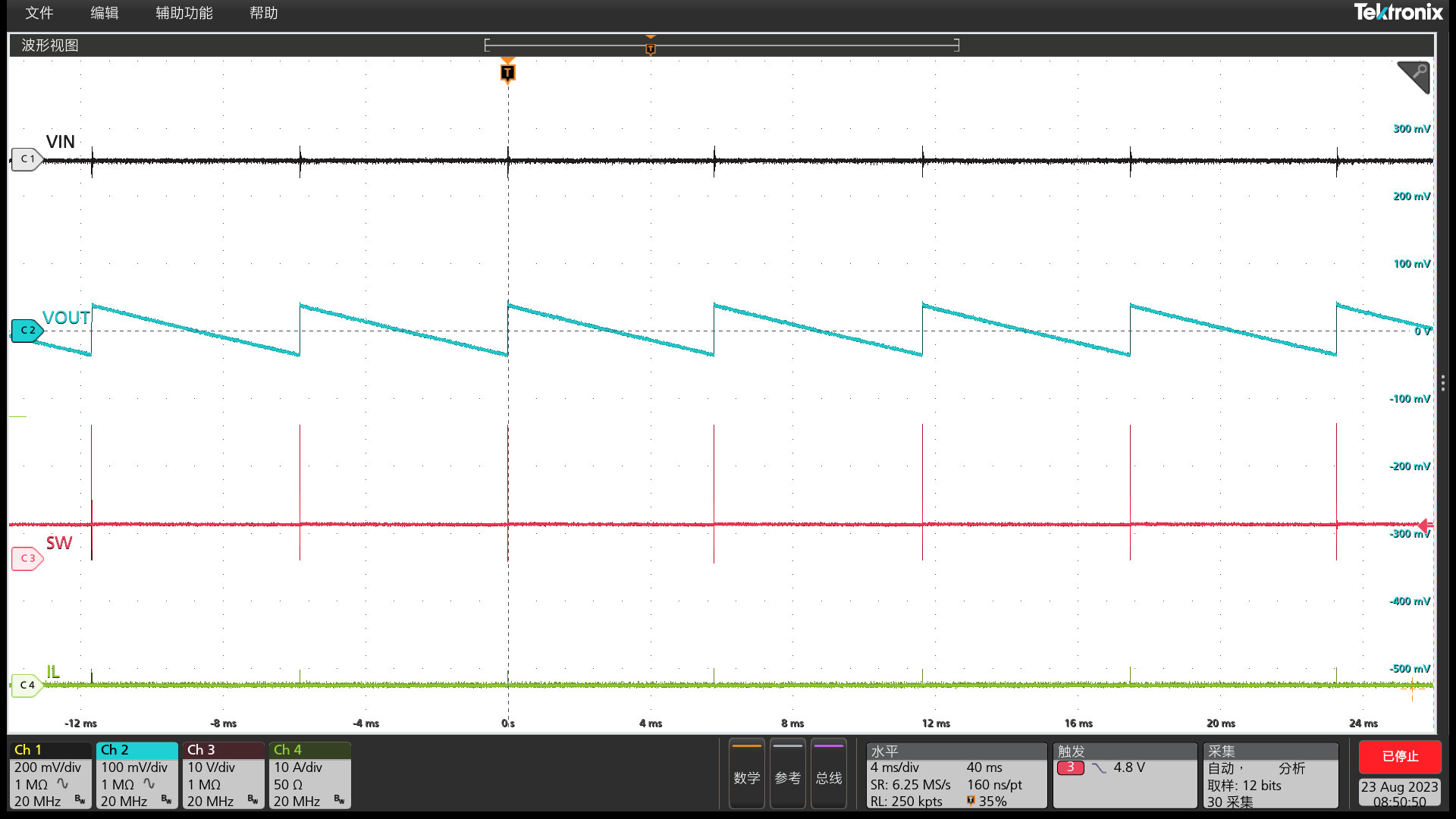 Figure 8-12 Output Voltage Ripple, Iout = 0 A, PSM Mode
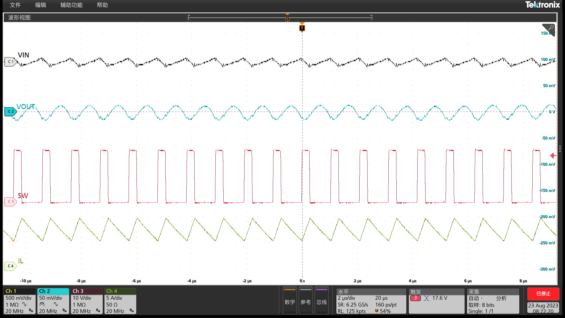 Figure 8-14 Output Voltage Ripple, Iout = 7 A
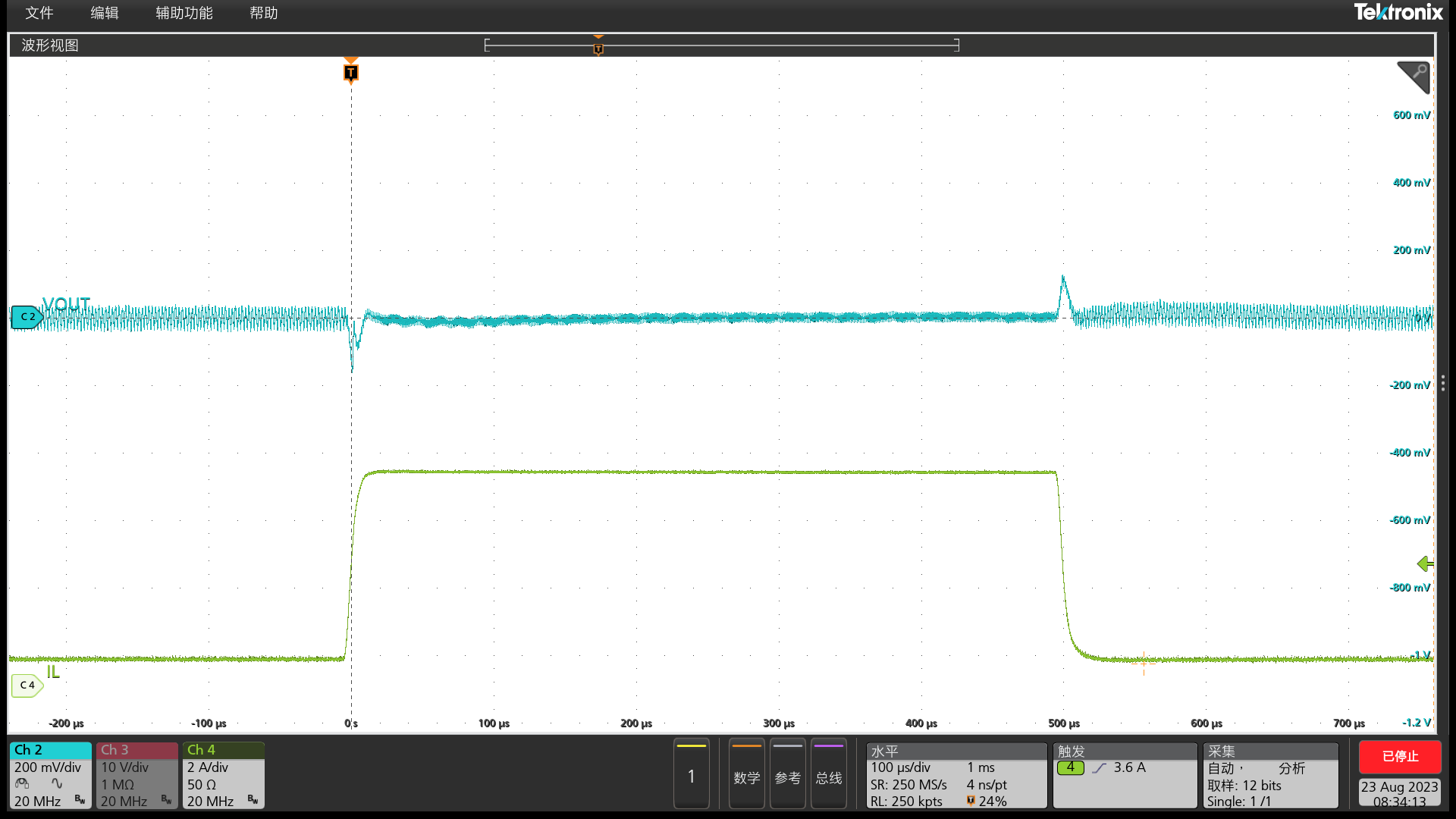 Figure 8-16 Transient Response, 0.7 A to 6.3 A with 2.5 A/us SR
 Figure 8-3 Efficiency, OOA Mode
 Figure 8-5 Switching Frequency, OOA Mode
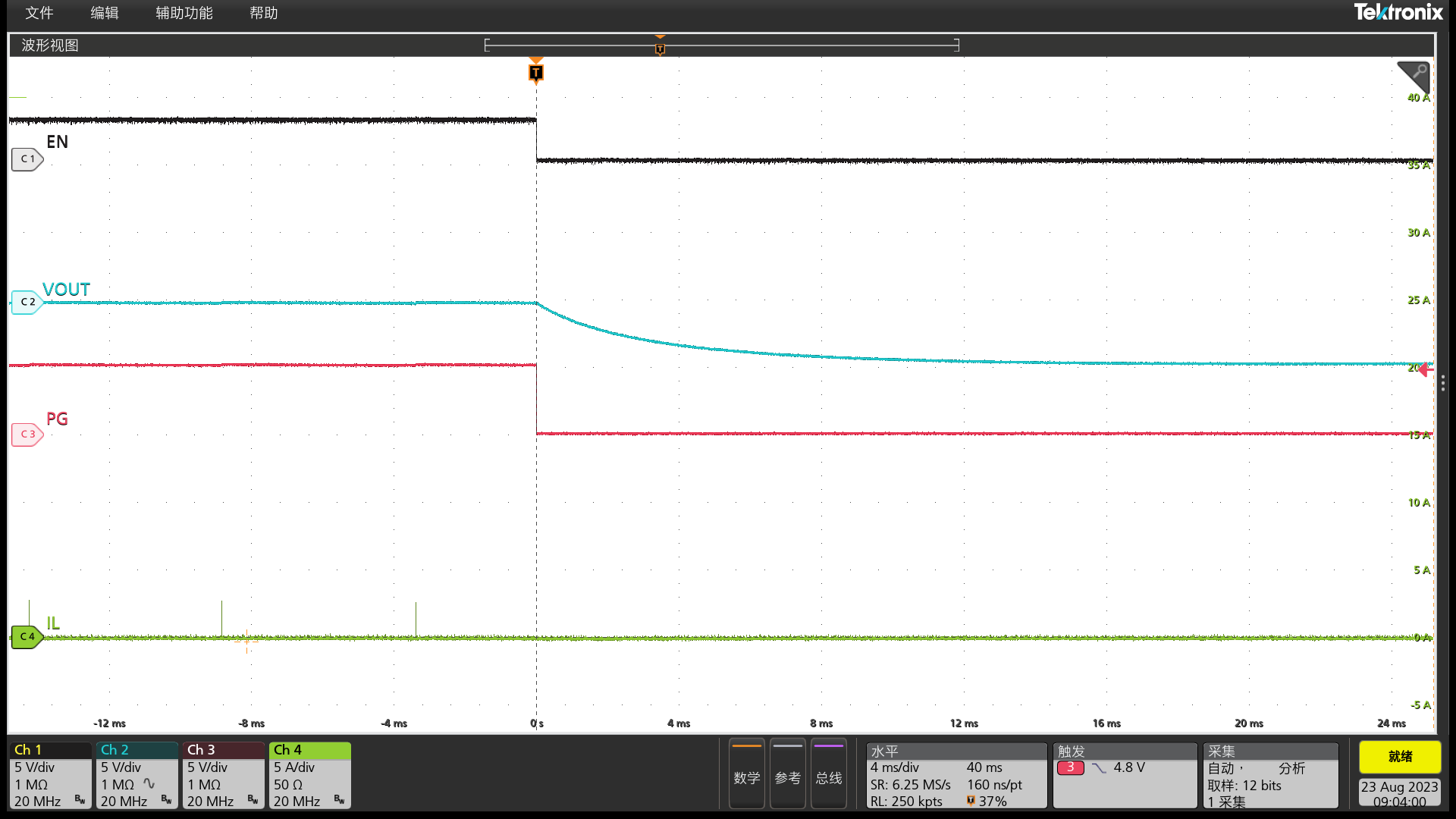 Figure 8-7 Shutdown Relative to EN Falling, Iout = 0A, PSM Mode
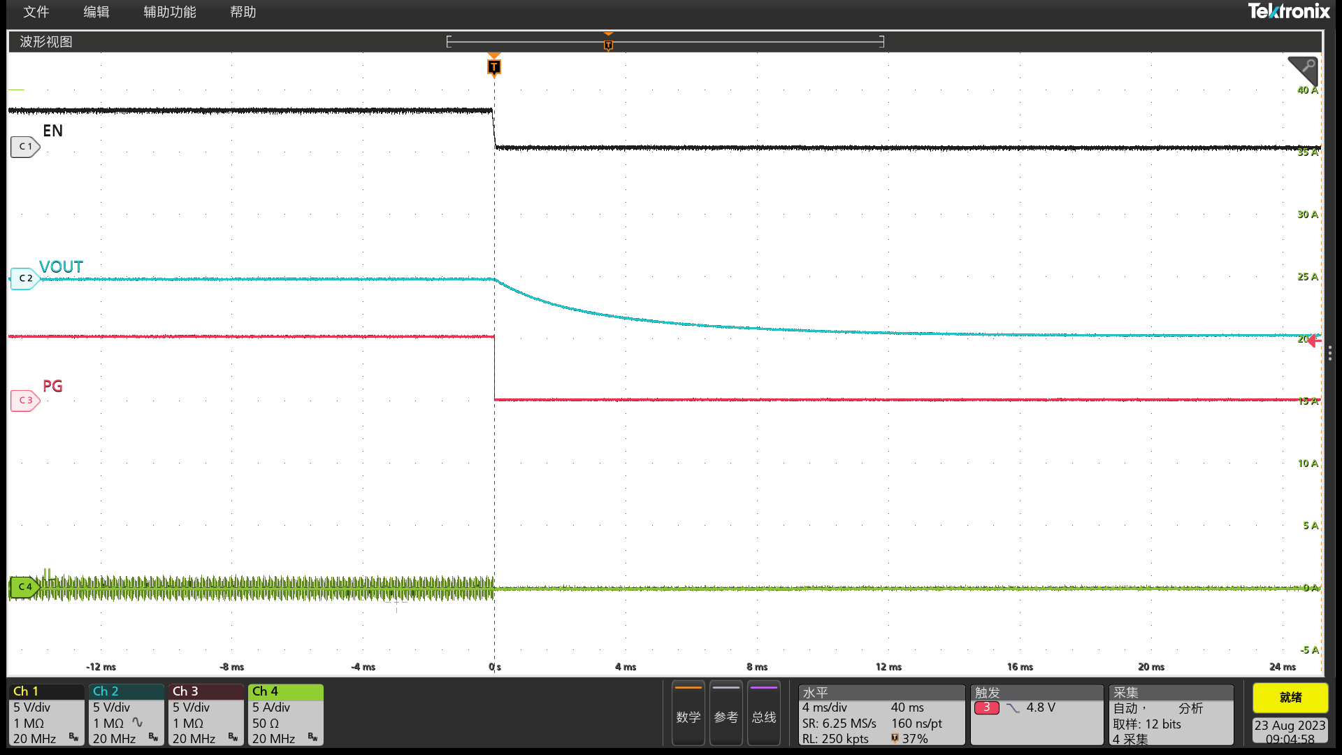 Figure 8-9 Shutdown Relative to EN Falling, Iout = 0A, OOA Mode
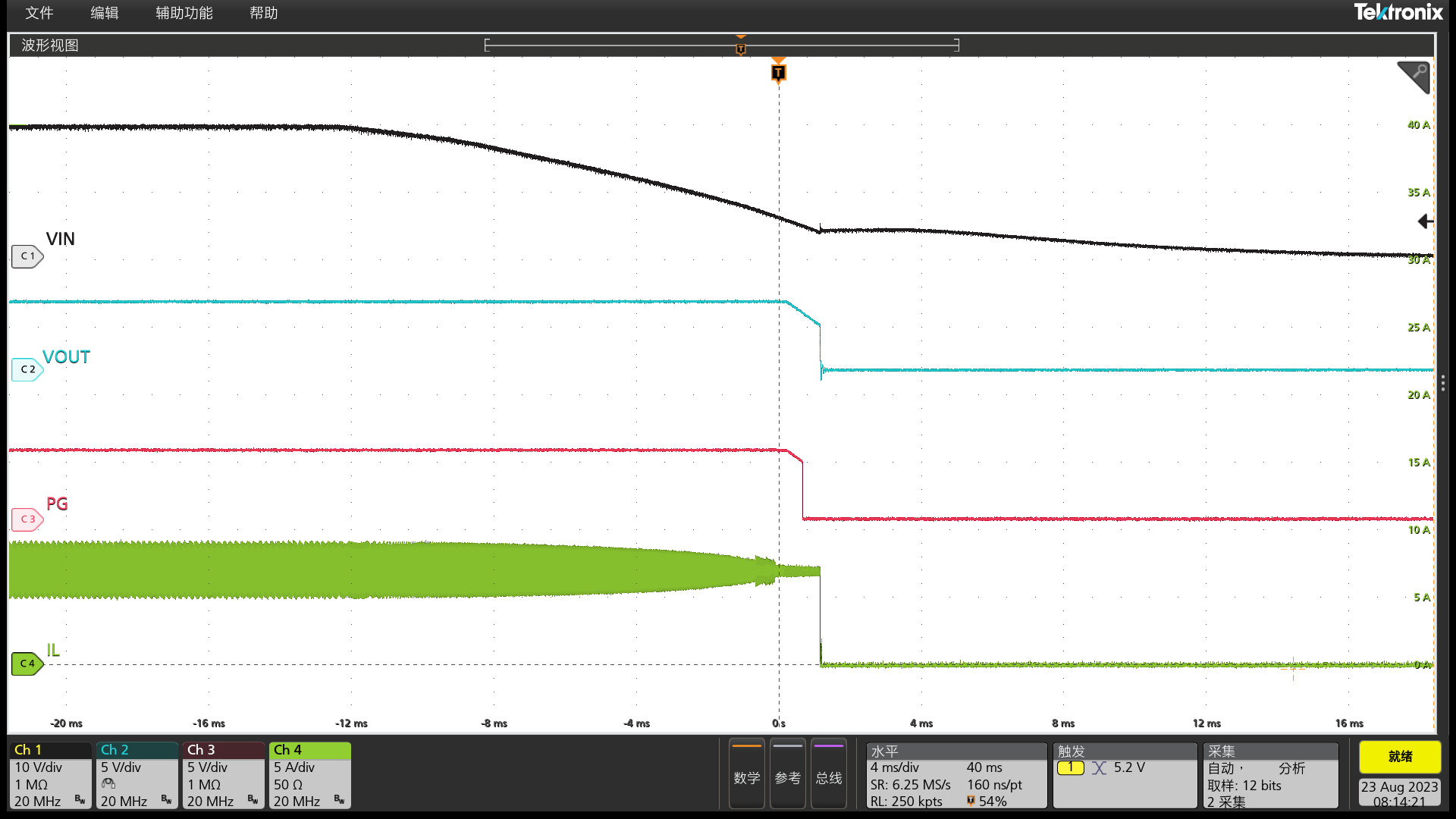 Figure 8-11 Shutdown Relative to Vin Falling, Iout = 7A
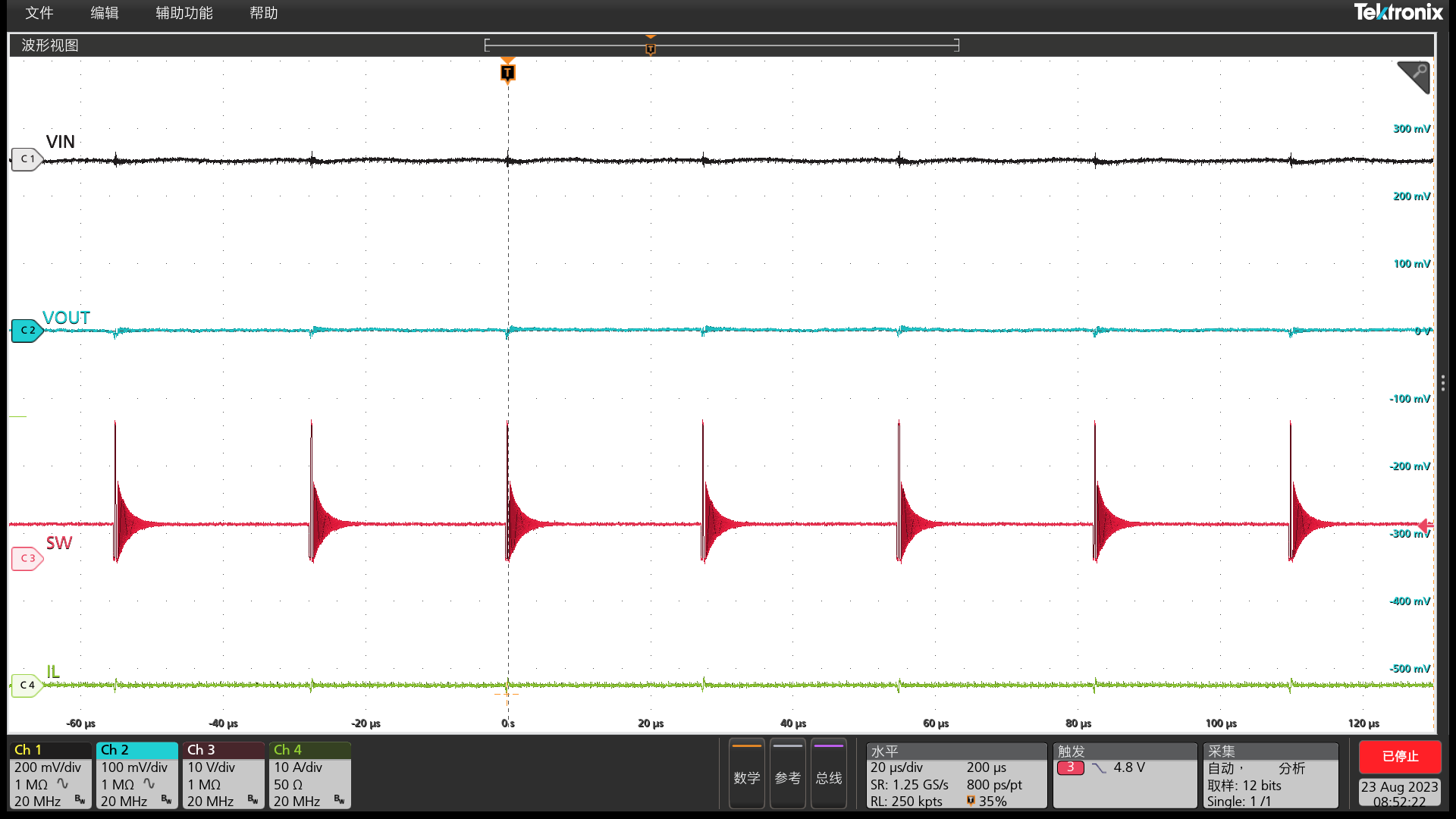 Figure 8-13 Output Voltage Ripple, Iout = 0 A, OOA Mode
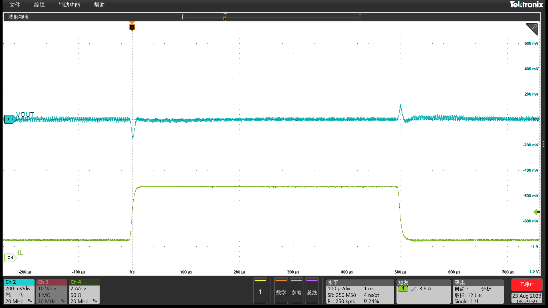 Figure 8-15 Transient Response, 1.4 A to 5.6 A with 2.5 A/us SR
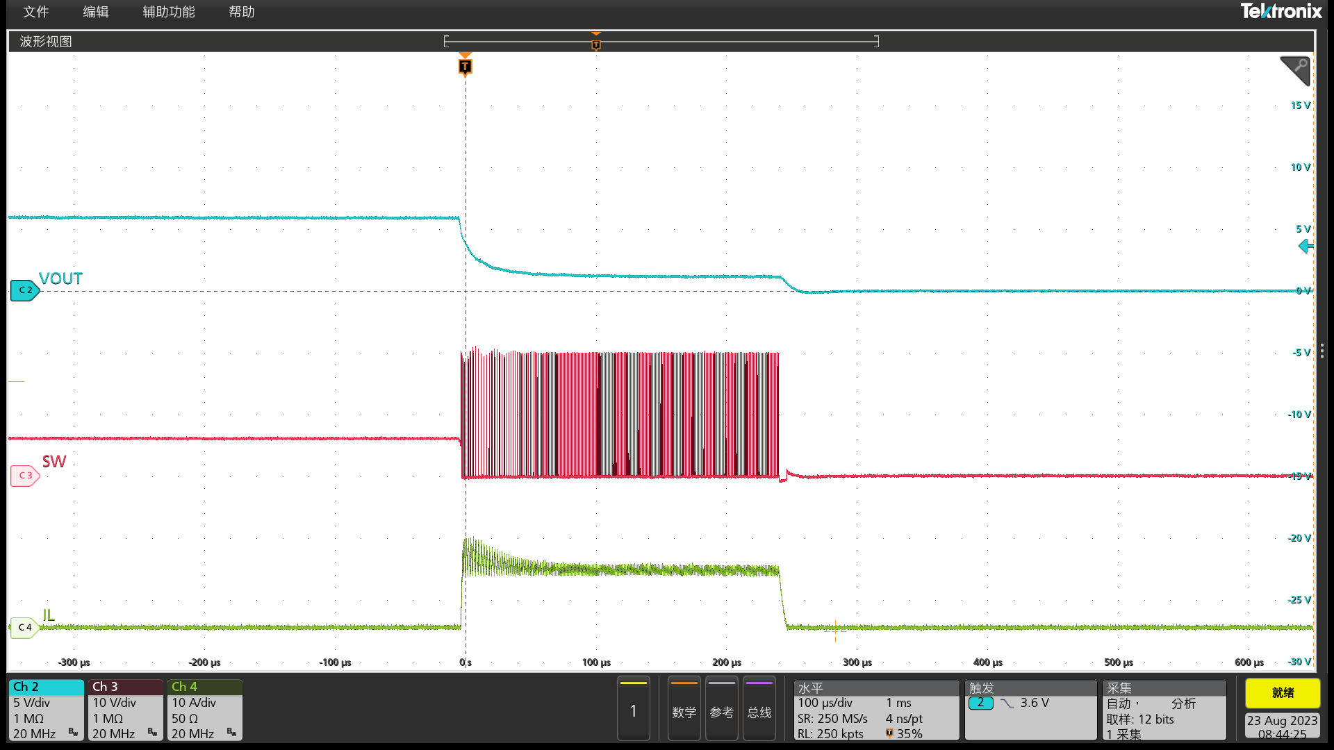 Figure 8-17 Normal Operation to Output Hard Short