JAJSJP3A September 2020 – October 2020 TPS51397A
PRODUCTION DATA
- 1 特長
- 2 アプリケーション
- 3 概要
- 4 Revision History
- 5 Pin Configuration and Functions
- 6 Specifications
- 7 Detailed Description
- 8 Application and Implementation
- 9 Power Supply Recommendations
- 10Layout
- 11Device and Documentation Support
- 12Mechanical, Packaging, and Orderable Information
7.4.4 Mode Selection
The device detects the voltage on the MODE pin during start-up and latches onto one of the MODE options listed in Table 7-1. The voltage on the MODE pin is recommended to be set by connecting this pin to the center tap of a resistor divider connected between VCC and AGND. A guideline for the top resistor (RM_H) and the bottom resistor (RM_L) as 1% resistors is shown in Table 7-1. It is recommended to choose the resistor to set the voltage at around the middle value of each range. It is important that the voltage for the MODE pin is derived from the VCC rail only since internally this voltage is referenced to detect the MODE option, and not to leave the mode pin floating. The MODE pin setting can be reset only by a VIN power cycling or EN toggle.
| VOLTAGE ON MODE | RM_H(kΩ) | RM_L (kΩ) | LIGHT LOAD OPERATION | FREQUENCY (kHz) |
|---|---|---|---|---|
| (0~10%)*VCC | 330 | 15 | Eco-mode | 500 |
| (10%~20%)*VCC |
180 |
33 | OOA | 500 |
| (20%~30%)*VCC | 160 | 51 | Eco-mode | 800 |
| (30%~50%)*VCC | 75 | 51 | OOA | 800 |
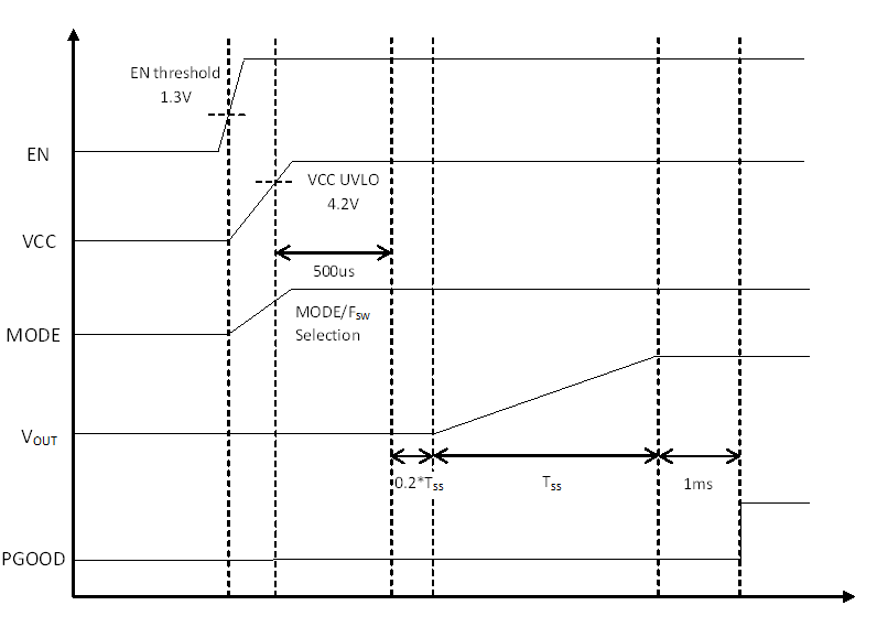
Figure 7-1 shows the typical start-up sequence of the device once the enable signal crosses the EN turnon threshold. After the voltage on VCC crosses the rising UVLO threshold, it takes about 500 μs to finish the working mode and frequency selection. The output voltage starts ramping after about 0.2*TSS delay time.
 Figure 7-1 Power-Up Sequence