JAJSJP3A September   2020  – October 2020 TPS51397A

PRODUCTION DATA  

  1. 特長
  2. アプリケーション
  3. 概要
  4. Revision History
  5. Pin Configuration and Functions
  6. Specifications
    1. 6.1 Absolute Maximum Ratings
    2. 6.2 ESD Ratings
    3. 6.3 Recommended Operating Conditions
    4. 6.4 Thermal Information
    5. 6.5 Electrical Characteristics
    6. 6.6 Typical Characteristics
  7. Detailed Description
    1. 7.1 Overview
    2. 7.2 Functional Block Diagram
    3. 7.3 Feature Description
      1. 7.3.1 PWM Operation and DCAP3 Control
      2. 7.3.2 Soft Start
      3. 7.3.3 Large Duty Operation
      4. 7.3.4 Power Good
      5. 7.3.5 Overcurrent Protection and Undervoltage Protection
      6. 7.3.6 Overvoltage Protection
      7. 7.3.7 UVLO Protection
      8. 7.3.8 Output Voltage Discharge
      9. 7.3.9 Thermal Shutdown
    4. 7.4 Device Functional Modes
      1. 7.4.1 Light Load Operation
      2. 7.4.2 Advanced Eco-mode Control
      3. 7.4.3 Out-of-Audio
      4. 7.4.4 Mode Selection
      5. 7.4.5 Standby Operation
  8. Application and Implementation
    1. 8.1 Application Information
    2. 8.2 Typical Application
      1. 8.2.1 Design Requirements
      2. 8.2.2 Detailed Design Procedure
        1. 8.2.2.1 External Component Selection
          1. 8.2.2.1.1 Output Voltage Set Point
          2. 8.2.2.1.2 MODE Selection
          3. 8.2.2.1.3 Inductor Selection
          4. 8.2.2.1.4 Output Capacitor Selection
          5. 8.2.2.1.5 Input Capacitor Selection
      3. 8.2.3 Application Curves
  9. Power Supply Recommendations
  10. 10Layout
    1. 10.1 Layout Guidelines
    2. 10.2 Layout Example
  11. 11Device and Documentation Support
    1. 11.1 Receiving Notification of Documentation Updates
    2. 11.2 サポート・リソース
    3. 11.3 Trademarks
    4. 11.4 静電気放電に関する注意事項
    5. 11.5 用語集
  12. 12Mechanical, Packaging, and Orderable Information

パッケージ・オプション

メカニカル・データ(パッケージ|ピン)
サーマルパッド・メカニカル・データ
発注情報

Layout Example

Figure 10-1 shows the recommended top-side layout. Component reference designators are the same as the circuit shown in Figure 8-1.
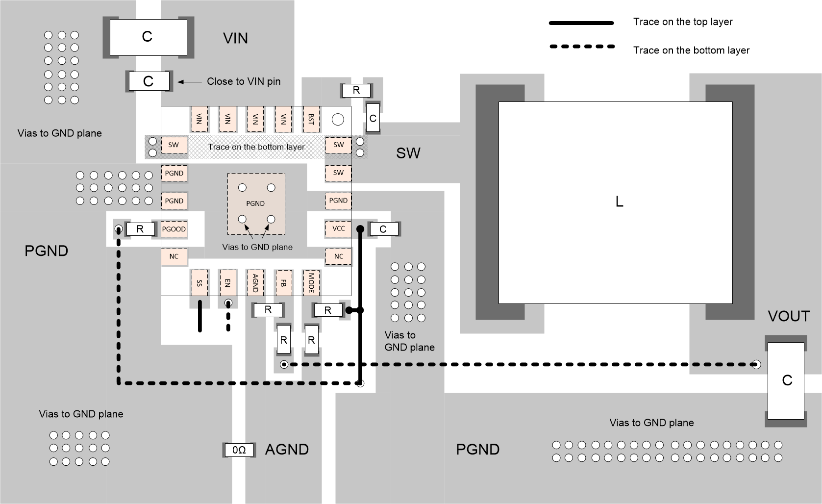
GUID-20200825-CA0I-LQPH-FVFJ-0X7CK3ZD9G4C-low.gif Figure 10-1 Top-Side Layout